1/10
October 2002
s
LOW "ON" RESISTANCE : 125
(Typ.)
OVER 15V p.p SIGNAL-INPUT RANGE FOR
V
DD
- V
EE
= 15V
s
HIGH "OFF" RESISTANCE : CHANNEL
LEAKAGE
±
100pA (Typ.) at V
DD
- V
EE
= 18V
s
BINARY ADDRESS DECODING ON CHIP
s
HIGH DEGREE OF LINEARITY : < 0.5%
DISTORTION TYP. at f
IS
= 1KHz, V
IS
= 5 V
pp
,
V
DD
- V
SS
> 10V, RL = 10K
s
VERY LOW QUIESCENT POWER
DISSIPATION UNDER ALL DIGITAL
CONTROL INPUT AND SUPPLY
CONDITIONS : 0.2
µ
W (Typ.)
at V
DD
- V
SS
= V
DD
- V
EE
=10V
s
MATCHED SWITCH CHARACTERISTICS :
R
ON
= 5
(Typ.) FOR V
DD
- V
EE
= 15V
s
WIDE RANGE OF DIGITAL AND ANALOG
SIGNAL LEVELS : DIGITAL 3 to 20,
ANALOG TO 20V p.p.
s
QUIESCENT CURRENT SPECIFIED UP TO
20V
s
5V, 10V AND 15V PARAMETRIC RATINGS
s
INPUT LEAKAGE CURRENT
I
I
= 100nA (MAX) AT V
DD
= 18V T
A
= 25°C
s
100% TESTED FOR QUIESCENT CURRENT
s
MEETS ALL REQUIREMENTS OF JEDEC
JESD13B " STANDARD SPECIFICATIONS
FOR DESCRIPTION OF B SERIES CMOS
DEVICES"
DESCRIPTION
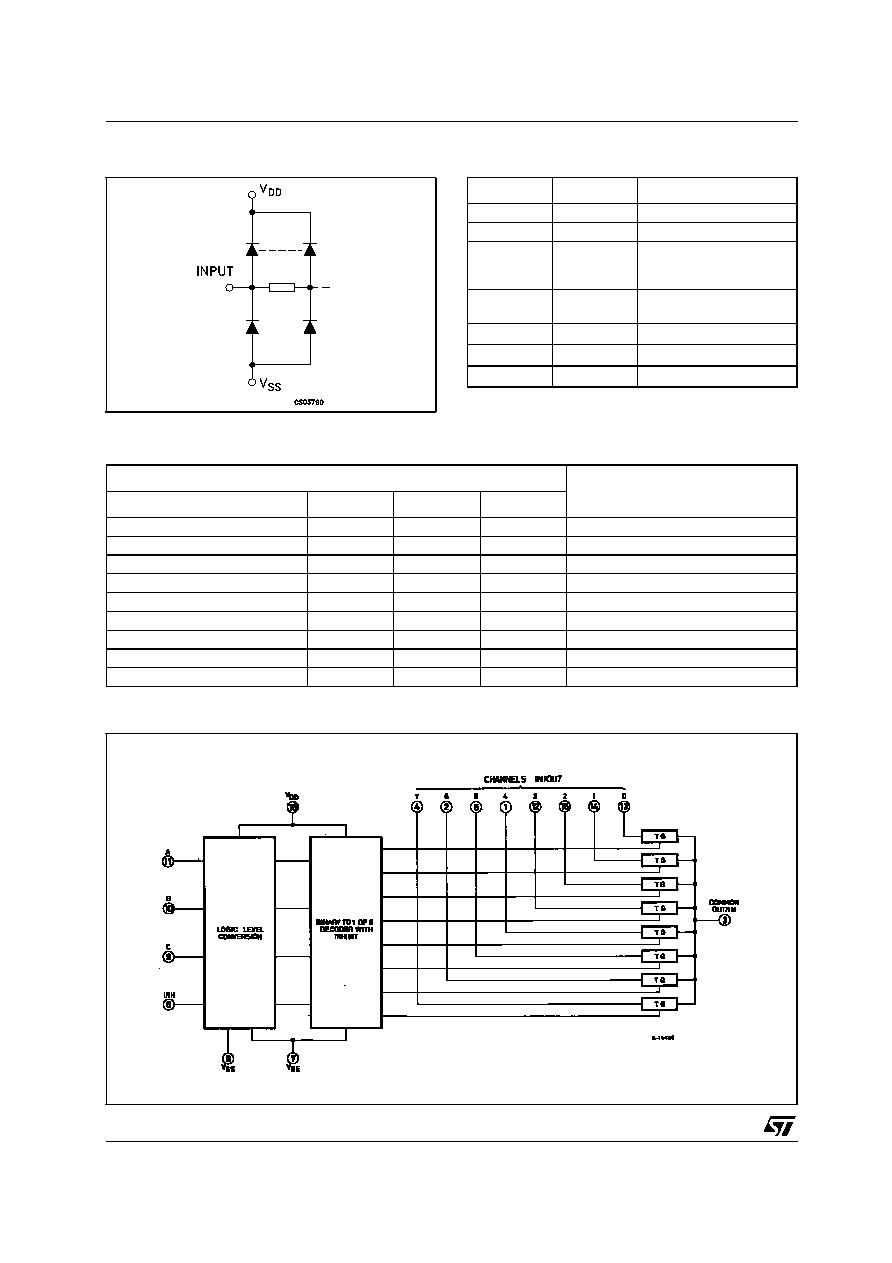
The HCF4051B is a monolithic integrated circuit
fabricated
in
Metal
Oxide
Semiconductor
technology available in DIP and SOP packages.
The HCF4051B analog multiplexer/demultiplexer
is a digitally controlled analog switch having low
ON impedance and very low OFF leakage current.
This multiplexer circuit dissipate extremely low
quiescent power over the full V
DD
- V
SS
and V
DD
-
V
EE
supply voltage range, independent of the
logic state of the control signals.
When a logic "1" is present at the inhibit input
terminal all channel are off. This device is a single
8-channel multiplexer having three binary control
inputs, A, B, and C, and an inhibit input. The three
binary signals select 1 of 8 channels to be turned
on, and connect one of the 8 inputs to the output.
HCF4051B
SINGLE 8-CHANNEL
ANALOG MULTIPLEXER/DEMULTIPLEXER
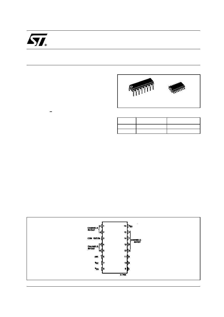
PIN CONNECTION
ORDER CODES
PACKAGE
TUBE
T & R
DIP
HCF4051BEY
SOP
HCF4051BM1
HCF4051M013TR
DIP
SOP
HCF4051B
3/10
ABSOLUTE MAXIMUM RATINGS
Absolute Maximum Ratings are those values beyond which damage to the device may occur. Functional operation under these conditions is
not implied.
All voltage values are referred to V
SS
pin voltage.
(*) 500mW at 65
°
C; derate to 300mW by 10mW/
°
C from 65
°
C to 85
°
C
RECOMMENDED OPERATING CONDITIONS
Symbol
Parameter
Value
Unit
V
DD
Supply Voltage
-0.5 to +22
V
V
I
DC Input Voltage
-0.5 to V
DD
+ 0.5
V
I
I
DC Input Current
±
10
mA
P
D
Power Dissipation per Package
500 (*)
mW
Power Dissipation per Output Transistor
100
mW
T
op
Operating Temperature
-55 to +125
°C
T
stg
Storage Temperature
-65 to +150
°C
Symbol
Parameter
Value
Unit
V
DD
Supply Voltage
3 to 20
V
V
I
Input Voltage
0 to V
DD
V
T
op
Operating Temperature
-55 to 125
°C
HCF4051B
4/10
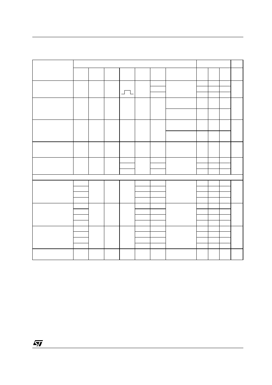
DC SPECIFICATIONS
* Determined by minimum feasible leakage measurement for automating testing.
Symbol
Parameter
Test Condition
Value
Unit
V
IS
(V)
V
EE
(V)
V
SS
(V)
V
DD
(V)
T
A
= 25°C
-40 to 85°C
-55 to 125°C
Min.
Typ.
Max.
Min.
Max.
Min.
Max.
I
L
Quiescent Device
Current (all
switches ON or all
switches OFF)
5
0.04
5
150
150
µ
A
10
0.04
10
300
300
15
0.04
20
600
600
20
0.08
100
3000
3000
SWITCH
R
ON
Resistance
0 < V
I
<
V
DD
0
0
5
470
1050
1200
1200
10
180
400
520
520
15
125
280
360
360
ON
Resistance
RON
(between any 2 of
4 switches)
0 < V
I
<
V
DD
0
0
5
10
10
10
15
5
OFF*
Channel Leakage
Current (All
Channel OFF)
(COMMON O/I)
0
0
18
±
0.1
100
1000
1000
nA
OFF*
Channel Leakage
Current (Any
Channel OFF)
0
0
18
±
0.1
100
1000
1000
nA
C
I
Input Capacitance
-5
-5
5
5
pF
C
O
Output
Capacitance
30
C
IO
Feedthrough
0.2
CONTROL (Address or Inhibit)
V
IL
Input Low Voltage
= VDD
thru
1K
V
EE
= V
SS
R
L
= 1K
to V
SS
I
IS
< 2
µ
A
(on all OFF
channels)
5
1.5
1.5
1.5
V
10
3
3
3
15
4
4
4
V
IH
Input High Voltage
5
3.5
3.5
3.5
V
10
7
7
7
15
11
11
11
I
IH,
I
IL
Input Leakage
Current
V
I
= 0/18V
18
±
10
-3
±
0.1
±
1
±
1
µ
A
C
I
Input Capacitance
5
7.5
pF
HCF4051B
5/10
DYNAMIC ELECTRICAL CHARACTERISTICS (T
amb
= 25°C, C
L
= 50pF, all input square wave rise and
fall time = 20 ns )
(1
)
Both ends of channel.
* Peak to Peak voltage symmetrical about (V
DD
- V
EE
) /2
Parameter
Test Condition
Value
Unit
V
EE
(V)
R
L
(K
)
f
I
(KHz)
V
I
(V)
V
SS
(V)
V
DD
(V)
Min. Typ. Max.
Propagation Delay
Time (signal input to
output)
200
V
DD
5
30
60
ns
10
15
30
15
11
20
Frequency Response
Channel "ON" (sine
wave input) at
20 log V
O
/V
I
= - 3dB
= V
SS
1
5(*)
10
V
O
at Common
OUT/IN
20
MHz
V
O
at any
channel
60
Feedthrough (all
channels OFF) at
20 log V
O
/V
I
= - 40dB
= V
SS
1
5(*)
10
V
O
at Common
OUT/IN
12
MHz
V
O
at any
channel
8
Frequency Signal
Crosstalk at
20 log V
O
/V
I
= -40dB
= V
SS
1
5(*)
10
Between any 2
channels
3
MHz
Sine Wave Distortion
f
IS
= 1KHz Sine Wave
= V
SS
10
1
2(*)
5
0.3
%
3(*)
10
0.2
5(*)
15
0.12
CONTROL (Address or Inhibit)
Propagation Delay:
Address to Signal
OUT (Channels ON
or OFF)
0
0
5
360
720
ns
0
0
10
160
320
0
0
15
120
240
-5
0
5
225
450
Propagation Delay:
Inhibit to Signal OUT
(Channel turning ON)
0
1
0
5
360
720
ns
0
0
10
160
320
0
0
15
120
240
-10
0
5
200
400
Propagation Delay:
Inhibit to Signal OUT
(Channel turning
OFF)
0
10
5
200
450
ns
0
10
90
210
0
15
70
160
-10
5
130
300
Address or Inhibit to
Signal Crosstalk
0
10
(1)
0
10
V
C
= V
DD
-V
SS
(square wave)
65
mV
peak