
1/10
September 2002
s
QUIESCENT CURRENT SPECIF. UP TO 20V
s
OPERATION OF LIQUID CRYSTALS WITH
CMOS CIRCUITS PROVIDES ULTRA LOW
POWER DISPLAY.
s
EQUIVALENT AC OUTPUT DRIVE FOR
LIQUID CRYSTAL DISPLAYS - NO
EXTERNAL CAPACITOR REQUIRED
s
VOLTAGE DOUBLING ACROSS DISPLAY
[(V
DD
- V
EE
) = 18V] RESULTS IN EFFECTIVE
36V (p-p) DRIVE ACROSS SELECTED
DISPLAY SEGMENTS
s
LOW OR HIGH OUTPUT LEVEL DC DRIVE
FOR OTHER TYPES OF DISPLAYS
s
ONE CHIP LOGIC LEVEL CONVERSION
FOR DIFFERENT INPUT AND OUTPUT
LEVEL SWINGS
s
FULL DECODING OF ALL INPUT
COMBINATIONS : "0 - 9, L, H, P, A" AND
BLANK POSITIONS
s
INPUT LEAKAGE CURRENT
I
I
= 100nA (MAX) AT V
DD
= 18V T
A
= 25�C
s
100% TESTED FOR QUIESCENT CURRENT
s
MEETS ALL REQUIREMENTS OF JEDEC
JESD13B "STANDARD SPECIFICATIONS
FOR DESCRIPTION OF B SERIES CMOS
DEVICES"
DESCRIPTION
HCF4056B is a monolithic integrated circuit
fabricated in Metal Oxide Semiconductor
technology available in DIP and SOP packages.
HCF4056B is a single digit BCD to 7 segment
decoder driver circuit that provides a level shifting
function on the chip. This feature permits the BCD
input-signal swings (V
DD
to V
SS
) to be the same
as or different from the 7-segment output signal
swings (V
DD
to V
EE
). For example, the BCD
input-signal swings (V
DD
to V
SS
) may be as low as
0 to -3V, whereas the output-display drive signal
swing (V
DD
to V
EE
) may be from 0 to -5V. If V
DD
to
V
EE
exceeds 15V, V
DD
to V
SS
should be at least
4V. The 7-segment outputs are controlled by the
DISPLAY-FREQUENCY (DF) input, which causes
the selected segment outputs to be low, high, or a
square wave output (for liquid crystal displays).
HCF4056B
BCD TO 7 SEGMENT DECODER /DRIVER
WITH STROBED LATCH FUNCTION
PIN CONNECTION
ORDER CODES
PACKAGE
TUBE
T & R
DIP
HCF4056BEY
SOP
HCF4056BM1
HCF4056M013TR
DIP
SOP

HCF4056B
2/10
INPUT EQUIVALENT CIRCUIT
PIN DESCRIPTION
FUNCTIONAL DIAGRAM
PIN No
SYMBOL
NAME AND FUNCTION
5, 3, 2, 4
2
0
, 2
1
, 2
2
, 2
3
BCD Inputs
9, 10, 11, 12,
13, 15, 14
a to g
7 - Segments Outputs
6
DISPLAY
FREQ. IN
Display Frequency Input
1
STROBE
Strobe Input
7
V
EE
Negative Supply Voltage
8
V
SS
Negative Supply Voltage
16
V
DD
Positive Supply Voltage
When the DF input is low, the output segments will
be high when selected by the BCD inputs. When
the DF input is high, the output segments will be
low when selected by the BCD inputs. When a
square wave is present at the DF input, the
selected segments will have a square wave output
that is 180
�
out of phase with the DF input. Those
segments which are not selected will have a
square wave output that is in phase with the input.
DF square wave repetition rates for liquid crystal
displays usually range from 30Hz (well above
flicker rate) to 200Hz (well below the upper limit of
the liquid crystal frequency response). HCF4056B
provides a strobed-latch function at the BCD
inputs. The decoding of all input combinations in
this device provides displays of 0 to 9 as well as L,
P, H, A, -, and a blank position. The level shifted
function permits the use of different input and
output signal swings. The input swings from a low
level of V
SS
to a high level of V
DD,
while the
outputs swing from a low level of V
EE
to the same
high level of V
DD
. Thus, the input and output
swings can be selected independently of each
other over a 3 to 18V range. V
SS
may be
connected to V
EE
when no level-shift function is
required. The HCF4056B, however must be used
together with HCF4054B to provide the common
DF output.
HCF4056B
3/10
TRUTH TABLE
ABSOLUTE MAXIMUM RATINGS
Absolute Maximum Ratings are those values beyond which damage to the device may occur. Functional operation under these conditions is
not implied.
All voltage values are referred to V
SS
pin voltage.
RECOMMENDED OPERATING CONDITIONS
INPUT CODE
OUTPUT STATE
DISPLAY
CHARACTER
2
3
2
2
2
1
2
0
a
b
c
d
e
f
g
L
L
L
L
H
H
H
H
H
H
L
0
L
L
L
H
L
H
H
L
L
L
L
1
L
L
H
L
H
H
L
H
H
L
H
2
L
L
H
H
H
H
H
H
L
L
H
3
L
H
L
L
L
H
H
L
L
H
H
4
L
H
L
H
H
L
H
H
L
H
H
5
L
H
H
L
H
L
H
H
H
H
H
6
L
H
H
H
H
H
H
L
L
L
L
7
H
L
L
L
H
H
H
H
H
H
H
8
H
L
L
H
H
H
H
H
L
H
H
9
H
L
H
L
L
L
L
H
H
H
L
L
H
L
H
H
L
H
H
L
H
H
H
H
H
H
L
L
H
H
L
L
H
H
H
P
H
H
L
H
H
H
H
L
H
H
H
A
H
H
H
L
L
L
L
L
L
L
H
-
H
H
H
H
L
L
L
L
L
L
L
BLANK
Symbol
Parameter
Value
Unit
V
DD
Supply Voltage
-0.5 to +22
V
V
I
DC Input Voltage
-0.5 to V
DD
+ 0.5
V
I
I
DC Input Current
�
10
mA
P
D
Power Dissipation per Package
200
mW
Power Dissipation per Output Transistor
100
mW
T
op
Operating Temperature
-55 to +125
�C
T
stg
Storage Temperature
-65 to +150
�C
Symbol
Parameter
Value
Unit
V
DD
Supply Voltage
3 to 20
V
V
I
Input Voltage
0 to V
DD
V
T
op
Operating Temperature
-55 to 125
�C

HCF4056B
4/10
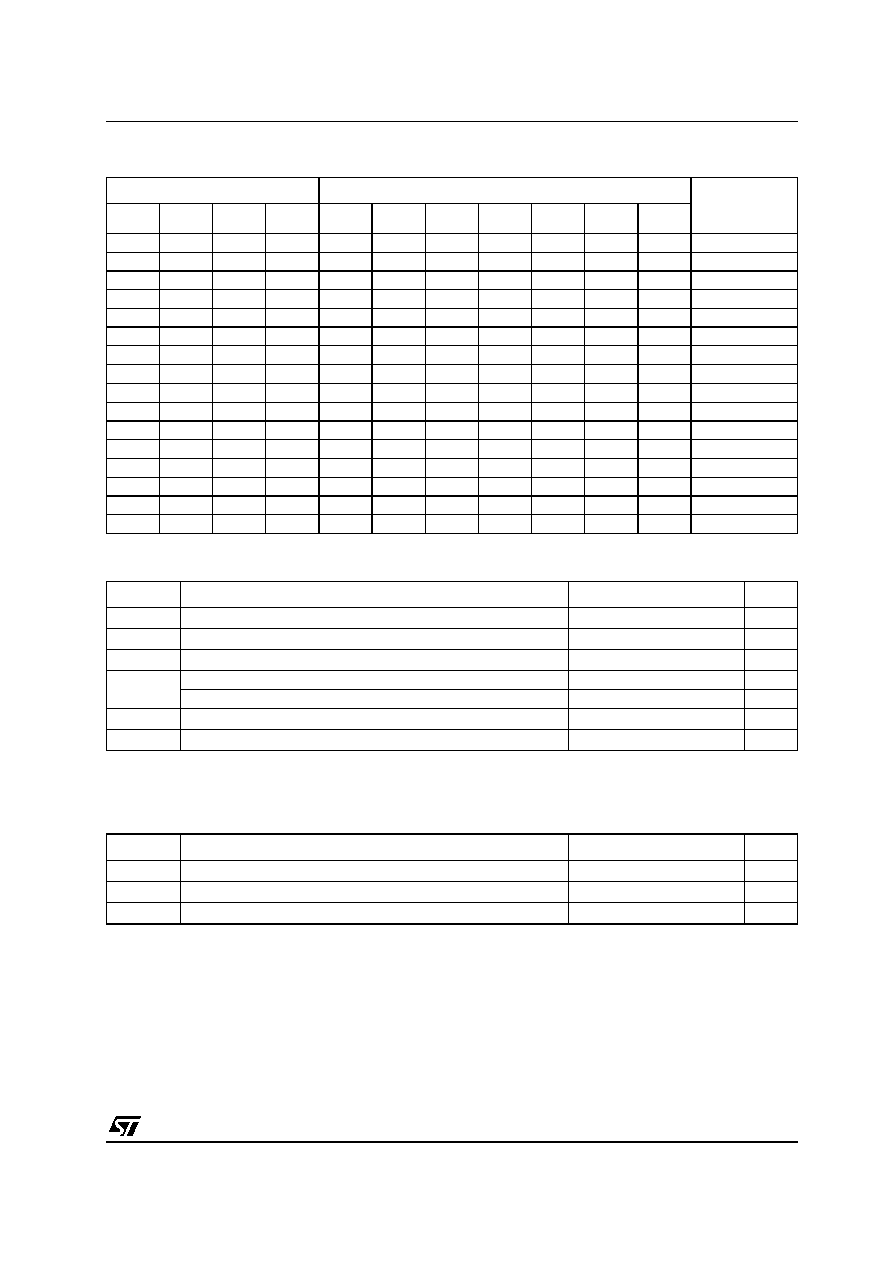
DC SPECIFICATIONS
The Noise Margin for both "1" and "0" level is: 1V min. with V
DD
=5V, 2V min. with V
DD
=10V, 2.5V min. with V
DD
=15V
DYNAMIC ELECTRICAL CHARACTERISTICS (T
amb
= 25�C, C
L
= 50pF, R
L
= 200K
, t
r
= t
f
= 20 ns)
(*) Typical temperature coefficient for all V
DD
value is 0.3 %/�C.
Symbol
Parameter
Test Condition
Value
Unit
V
EE
(V)
V
I
(V)
V
O
(V)
V
SS
(V)
V
DD
(V)
T
A
= 25�C
-40 to 85�C -55 to 125�C
Min.
Typ.
Max.
Min.
Max.
Min.
Max.
I
L
Quiescent Current
-5
0/5
0
5
0.04
5
150
150
�
A
0
0/10
0
10
0.04
10
300
300
0
0/15
0
15
0.04
20
600
600
0
0/20
0
20
0.08
100
3000
3000
V
OH
High Level Output
Voltage
0
0/5
0
5
4.95
4.95
4.95
V
0
0/10
0
10
9.95
9.95
9.95
0
0/15
0
15
14.95
14.95
14.95
V
OL
Low Level Output
Voltage
0
5/0
0
5
0.05
0.05
0.05
V
0
10/0
0
10
0.05
0.05
0.05
0
15/0
0
15
0.05
0.05
0.05
V
IH
High Level Input
Voltage
-5
0.5/4.5
0
5
3.5
3.5
3.5
V
0
1/9
0
10
7
7
7
0
1.5/18.5
0
15
11
11
11
V
IL
Low Level Input
Voltage
5
0.5/4.5
0
5
1.5
1.5
1.5
V
0
9/1
0
10
3
3
3
0
1.5/18.5
0
15
4
4
4
I
OH
Output Drive
Current
-5
0/5
4.5
0
5
-0.38
-0.9
-0.28
-0.28
mA
0
0/10
9.5
0
10
-0.38
-0.9
-0.28
-0.28
0
0/15
13.5
0
15
-1.27
-3
-0.95
-0.95
I
OL
Output Sink
Current
-5
0/5
0.4
0
5
1.1
2.6
0.82
0.82
mA
0
0/10
0.5
0
10
1.1
2.6
0.82
0.82
0
0/15
1.5
0
15
2.9
6.8
2.17
2.17
I
I
Input Leakage
Current (any input)
0
0/18
0
18
�
10
-5
�
0.1
�
1
�
1
�
A
C
I
Input Capacitance
(any input)
5
7.5
pF
Symbol
Parameter
Test Condition
Value (*)
Unit
V
EE
(V)
V
SS
(V)
V
DD
(V)
Min.
Typ.
Max.
t
PHL
t
PLH
Propagation Delay
Time (any Input to
any Output)
-5
0
5
650
1300
ns
0
0
10
575
1150
0
0
15
375
750
t
THL
t
TLH
Transition Time
(any Output)
-5
0
5
100
200
ns
0
0
10
100
200
0
0
15
75
150

HCF4056B
5/10
TYPICAL APPLICATIONS
FIGURE 1 : Display Driver Circuit
FIGURE 2 : Display Driver Waveforms.