HCC/HCF4098B
DUAL MONOSTABLE MULTIVIBRATOR
.
RETRIGGERABLE/RESETTABLE CAPABILITY
.
TRIGGER AND RESET PROPAGATION DE-
LAYS INDEPENDENT OF R
X
, C
X
.
TRIGGERING FROM LEADING OR TRAILING
EDGE
.
Q AND Q BUFFERED OUTPUTS AVAILABLE
.
SEPARATE RESETS
.
WIDE RANGE OF OUTPUT-PULSE WIDTHS
.
QUIESCENT CURRENT SPECIFIED TO 20V
FOR HCC DEVICE
.
5V, 10V, AND 15V PARAMETRIC RATINGS
.
INPUT
CURRENT OF 100nA AT 18V AND
25
∞
C FOR HCC DEVICE
.
100% TESTED FOR QUIESCENT CURRENT
.
MEETS ALL REQUIREMENTS OF JEDEC TEN-
TATIVE STANDARD N
∞
13A, "STANDARD
SPECIFICATIONS FOR DESCRIPTION OF "B"
SERIES CMOS DEVICES"
June 1989
The HCC4098B (extended temperature range) and
HCF4098B (intermediate temperature range) are
monolithic integrated circuit, available in 16-lead
dual in-line dual in-line plastic or ceramic package
and plastic micropackage. The HCC/HCF4098B
dual monostable multivibrator provides stable retrig-
gerable/resettable one-shot operation for any fixed-
voltage timing application. An external resistor (R
X
)
and an external capacitor (C
X
) control the timing for
the circuit. Adjustment of R
X
and C
X
provides a wide
range of output pulse widths from the Q and Q ter-
minals. The time delay from trigger input to output
transition (trigger propagation delay) and the time
delay from reset input to output transition (reset pro-
pagation delay) are independent of R
X
and C
X
.
Leading-edge-triggering (+ TR) and trailing-edge-
triggering (≠ TR) inputs are provided for triggering
from either edge of an input pulse. An unused + TR
input should be tied to V
SS
. An unused ≠ TR input
should be tied to V
DD
. A RESET (on low level) is pro-
vided for immediate termination of the output pulse
or to prevent output pulses when power is turned on.
An unused RESET input should be tied to V
DD
. How-
ever, if an entire section of the 4098B is not used,
its RESET should be tied to V
SS
. See table I. In nor-
mal operation the circuit triggers (extends the output
EY
(Plastic Package)
F
(Ceramic Frit Seal Package)
C1
(Plastic Chip Carrier)
ORDER CODES :
HCC4098BF
HCF4098BM1
HCF4098BEY
HCF4098BC1
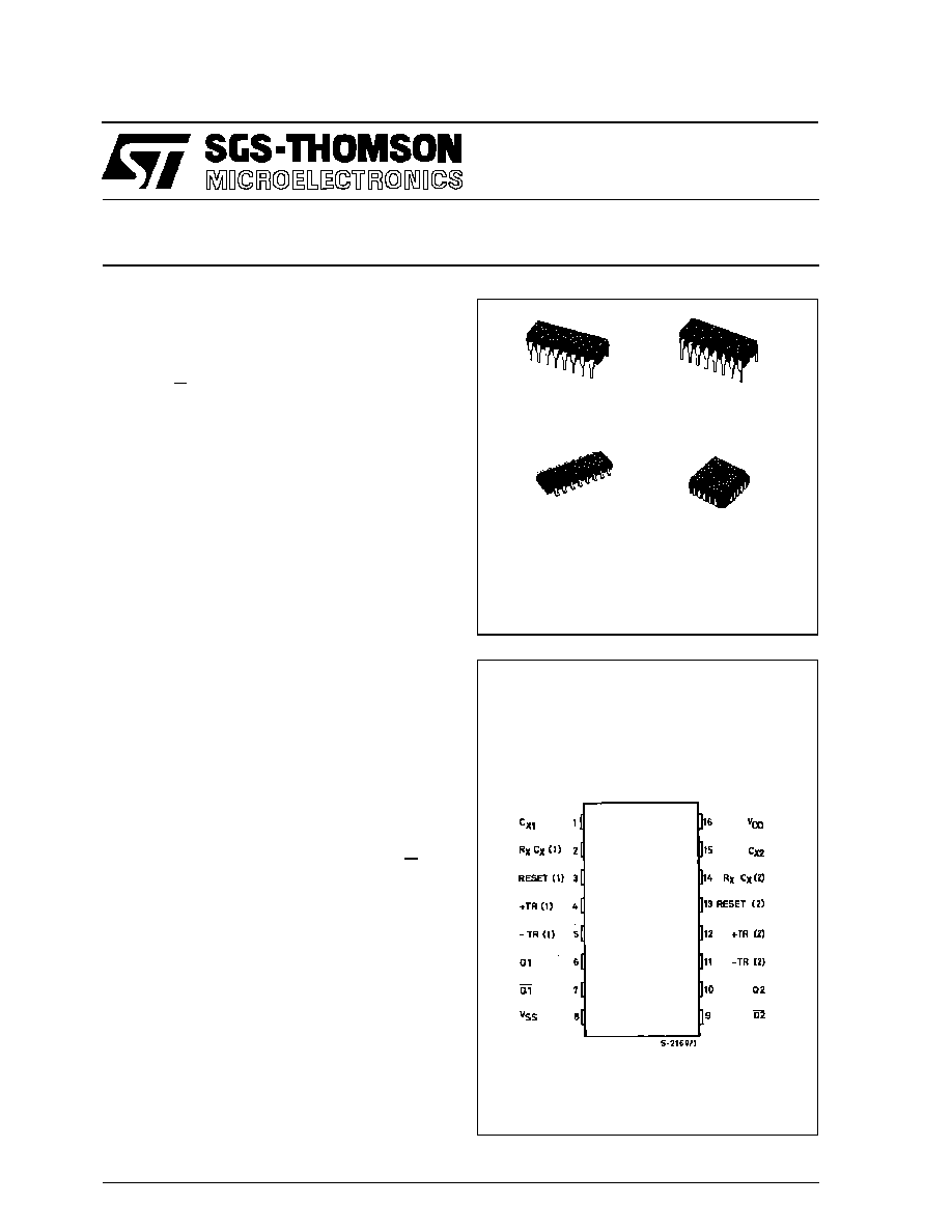
PIN CONNECTIONS
M1
(Micro Package)
DESCRIPTION
1/14

FUNCTIONAL DIAGRAM
ABSOLUTE MAXIMUM RATINGS
Symbol
Parameter
Value
Unit
V
DD
*
Supply Voltage : HC C Types
H C F Types
≠ 0.5 to + 20
≠ 0.5 to + 18
V
V
V
i
Input Voltage
≠ 0.5 to V
DD
+ 0.5
V
I
I
DC Input Current (any one input)
±
10
mA
P
t o t
Total Power Dissipation (per package)
Dissipation per Output Transistor
for T
o p
= Full Package-temperature Range
200
100
mW
mW
T
o p
Operating Temperature : HCC Types
H CF Types
≠ 55 to + 125
≠ 40 to + 85
∞
C
∞
C
T
s t g
Storage Temperature
≠ 65 to + 150
∞
C
RECOMMENDED OPERATING CONDITIONS
Symbol
Parameter
Value
Unit
V
DD
Supply Voltage : HC C Types
H CF Types
3 to 18
3 to 15
V
V
V
I
Input Voltage
0 to V
DD
V
T
o p
Operating Temperature : HCC Types
H CF Types
≠ 55 to + 125
≠ 40 to + 85
∞
C
∞
C
Stresses above those listed under "Absolute Maximum Ratings" may cause permanent damage to the device. This is a stress rating only
and functional operation of the device at these or any other conditions above those indicated in the operational sections of this specification
is not implied. Exposure to absolute maximum rating conditions for external periods may affect device reliability.
* All voltage values are referred to V
SS
pin voltage.
pulse one period) on the application of each new
trigger pulse. For operation in the non-triggerable
mode, Q is connected to ≠TR when leading-edge
triggering (+ TR) is used or Q is connected to + TR
when trailing-edge triggering (≠ TR) is used. The time
period (T) for this multivibrator can be approximated
by T
X
=
1/2
R
X
C
X
for C
X
0.01
µ
F. Time periods as
a function of R
X
for values of C
X
and V
DD
are given in
fig. 8. Values of T vary from unit to unit and as a func-
tion of voltage, temperature, and R
X
C
X
. The minimum
value of external resistance, R
X
, is 5 k
. The maxi-
mum value of external capacitance, C
X
, is 100
µ
F.
Fig.9 shows time periods as a function of C
X
forvalues
of R
X
and V
DD
. The output pulse width has vari-
ations of
±
2.5 % typically, over the temperature range
of ≠ 55
∞
C to 125
∞
C for C
X
= 1000pF and R
X
= 100
k
. For power supply variations of
±
5%, the output
pulse width has variations of
±
0.5% typically, for V
DD
= 10V and 15V and
±
1% typically, for V
DD
= 5 V at
C
X
= 1000 pF and R
X
= 5k
.
HCC/HCF4098B
2/14

LOGIC DIAGRAMS
Table 1 : Functional Terminal Connections.
Termi nal Connections
to V
D D
to V
S S
Input Pulse to
Other
Connections
Function
Mono
( 1 )
Mono
( 2 )
Mono
( 1 )
Mono
( 2 )
Mono
( 1 )
Mono
( 2 )
Mono
( 1 )
Mono
( 2 )
Leading - Edge
Trigger/Retriggerable
3,5
11,13
4
12
Leading - Edge
Trigger/Non - retriggerable
3
13
4
12
5,7
11,9
Trailing - Edge
Trigger/Retriggerable
3
13
4
12
5
11
Trailing - Edge
Trigger/Non - retriggerable
3
13
5
11
4,6
12,10
Unused Section
5
11
3,4
12,13
Notes : 1. A Refriggerable one-shot multivibrator has an output pulse width which is extended one full time period (T
X
) after application of the
last trigger pulse.
2. A non-refriggerable one-shot multivibrator has a time period T
X
referenced from the application of the first trigger pulse.
HCC/HCF4098B
3/14

STATIC ELECTRICAL CHARACTERISTICS (over recommended operating conditions)
Test Conditions
Val ue
V
I
V
O
|I
O
|
V
D D
T
L o w
*
25
∞
C
T
Hi g h
*
Symbol
Parameter
(V)
(V)
(
µ
A)
(V)
Min. Max. Min. Typ. Max. Min. Max.
Unit
I
L
Quiescent
Current
HCC
Types
0/ 5
5
1
0.02
1
30
µ
A
0/10
10
2
0.02
2
60
0/15
15
4
0.02
4
120
0/20
20
20
0.04
20
600
HCF
Types
0/ 5
5
4
0.02
4
30
0/10
10
8
0.02
8
60
0/15
15
16
0.02
16
120
V
O H
Output High
Voltage
0/ 5
< 1
5
4.95
4.95
4.95
V
0/10
< 1
10
9.95
9.95
9.95
0/15
< 1
15
14.95
14.95
14.95
V
O L
Output Low
Voltage
5/0
< 1
5
0.05
0.05
0.05
V
10/0
< 1
10
0.05
0.05
0.05
15/0
< 1
15
0.05
0.05
0.05
V
IH
Input High
Voltage
0.5/4.5
< 1
5
3.5
3.5
3.5
V
1/9
< 1
10
7
7
7
1.5/13.5
< 1
15
11
11
11
V
IL
Input Low
Voltage
4.5/0.5
< 1
5
1.5
1.5
1.5
V
9/1
< 1
10
3
3
3
13.5/1.5
< 1
15
4
4
4
I
O H
Output
Drive
Current
HCC
Types
0/ 5
2.5
5
≠ 2
≠ 1.6 ≠ 3.2
≠ 1.15
mA
0/ 5
4.6
5
≠ 0.64
≠ 0.51 ≠ 1
≠ 0.36
0/10
9.5
10
≠ 1.6
≠ 1.3 ≠ 2.6
≠ 0.9
0/15
13.5
15
≠ 4.2
≠ 3.4 ≠ 6.8
≠ 2.4
HCF
Types
0/ 5
2.5
5
≠ 1.53
≠ 1.36 ≠ 3.2
≠ 1.1
0/ 5
4.6
5
≠ 0.52
≠ 0.44 ≠ 1
≠ 0.36
0/10
9.5
10
≠ 1.3
≠ 1.1 ≠ 2.6
≠ 0.9
0/15
13.5
15
≠ 3.6
≠ 3.0 ≠ 6.8
≠ 2.4
I
O L
Output
Sink
Current
HCC
Types
0/ 5
0.4
5
0.64
0.51
1
0.36
mA
0/10
0.5
10
1.6
1.3
2.6
0.9
0/15
1.5
15
4.2
3.4
6.8
2.4
HCF
Types
0/ 5
0.4
5
0.52
0.44
1
0.36
0/10
0.5
10
1.3
1.1
2.6
0.9
0/15
1.5
15
3.6
3.0
6.8
2.4
I
IH
, I
IL
Input
Leakage
Current
HCC
Types
0/18
Any Input
18
±
0.1
±
10
≠ 5
±
0.1
±
1
µ
A
HCF
Types
0/15
15
±
0.3
±
10
≠ 5
±
0.3
±
1
C
I
Input Capacitance
Any Input
5
7.5
pF
* T
Low
= ≠ 55
∞
C for HCC device : ≠ 40
∞
C for HCF device.
* T
High
= + 125
∞
C for HCC device : + 85
∞
C for HCF device.
The Noise Margin for both "1" and "0" level is : 1V min. with V
DD
= 5V, 2V min. with V
DD
= 10V, 2.5 V min. with V
DD
= 15V.
HCC/HCF4098B
4/14

DYNAMIC ELECTRICAL CHARACTERISTICS (T
amb
= 25
∞
C, C
L
= 50pF, R
L
= 200k
,
typical temperature coefficient for all V
DD
values is 0.3%/
∞
C, all input rise and fall times = 20ns)
Test Conditions
Val ue
Symbol
Parameter
R
X
(k
)
C
X
(pF)
V
D D
(V)
Min.
Typ.
Max.
Unit
t
P L H
, t
P HL
Trigger Propagation Delay Time
(+ TR, ≠ TR to Q, Q)
5 to 10.000
15
5
250
500
ns
10
125
250
15
100
200
t
WH
, t
WL
Trigger Pulse Width
5 to 10.000
15
5
140
70
ns
10
60
30
15
40
20
t
T L H
Transition Time
5 to 10.000
15
5
100
200
ns
10
50
100
15
40
80
t
T HL
Transition Time
5 to 10.000 15 to 10.000
5
100
200
10
50
100
15
40
80
5 to 10.000
0.01
µ
F
to 0.1
µ
F
5
150
300
10
75
150
15
65
130
5 to 10.000
0.1
µ
F
to 1
µ
F
5
250
500
10
150
300
15
80
160
t
P L H
, t
P HL
Propagation Delay Time (reset)
5 to 10.000
15
5
225
450
ns
10
125
250
15
75
150
t
W
R
Pulse Width (reset)
100
15
5
200
100
ns
10
80
40
15
60
30
1000
5
1200
600
10
600
300
15
500
250
0.1
µ
F
5
50
250
µ
s
10
30
15
15
20
10
t
r
, t
f
(TR)
Rise or Fall Time (trigger)
5 to 15
100
µ
s
Pulse Width Match Between
Circuits in Same Package
10
10.000
5
5
10
%
10
7.5
15
15
7.5
15
HCC/HCF4098B
5/14