 | –≠–ª–µ–∫—Ç—Ä–æ–Ω–Ω—ã–π –∫–æ–º–ø–æ–Ω–µ–Ω—Ç: HCF4541 | –°–∫–∞—á–∞—Ç—å:  PDF PDF  ZIP ZIP |
HCC4541B
HCF4541B
November 1996
PROGRAMMABLE TIMER
EY
(Plastic Package)
16 STAGE BINARI COUNTER
LOW SYMMETRICAL OUTPUT RESISTANCE,
TYPICALLY 100 OHM AT V
DD
= 15V
OSCILLATOR FREQUENCY RANGE : DC TO
100kHz
AUTO OR MASTER RESET DISABLES OSCIL-
LATOR DURING RESET TO REDUCE POWER
DISSIPATION
OPERATES WITH VERY SLOW CLOCK RISE
AND FALL TIMES
BUILT-IN LOW-POWER RC OSCILLATOR
EXTERNAL CLOCK (applied to pin 3) CAN BE
USED INSTEAD OF OSCILLATOR
OPERATES AS 2
N
FREQUENCY DIVIDER OR
AS A SINGLE-TRANSITION TIMER
Q/Q SELECT PROVIDES OUTPUT LOGIC
LEVEL FLEXIBILITY
CAPABLE OF DRIVING SIX LOW POWER TTL
LOADS, THREE LOW-POWER SCHOTTKY
LOADS, PR SIX HTL LOADS OVER THE
RATED TEMPERATURE RANGE
SYMMETRICAL
OUTPUT
CHARAC-
TERISTICS
100% TESTED FOR QUIESCENT CURRENT
AT 20V
5-10-15V PARAMETRIC RATINGS
MEETS ALL REQUIREMENTS OF JEDEC TEN-
TATIVE STANDARD N 13A, "STANDARD SPE-
CIFICATIONS FOR DESCRIPTION OF ' B '
SERIES CMOS DEVICES"
ORDER CODES :
HCC4541 BF
HCF4541 BM1
HCF4541 BEY
HCF4541 BC1
F
(Ceramic Frit Seal Package)
M1
(Micro Package)
C1
(Plastic Chip Carrier)
DESCRIPTION
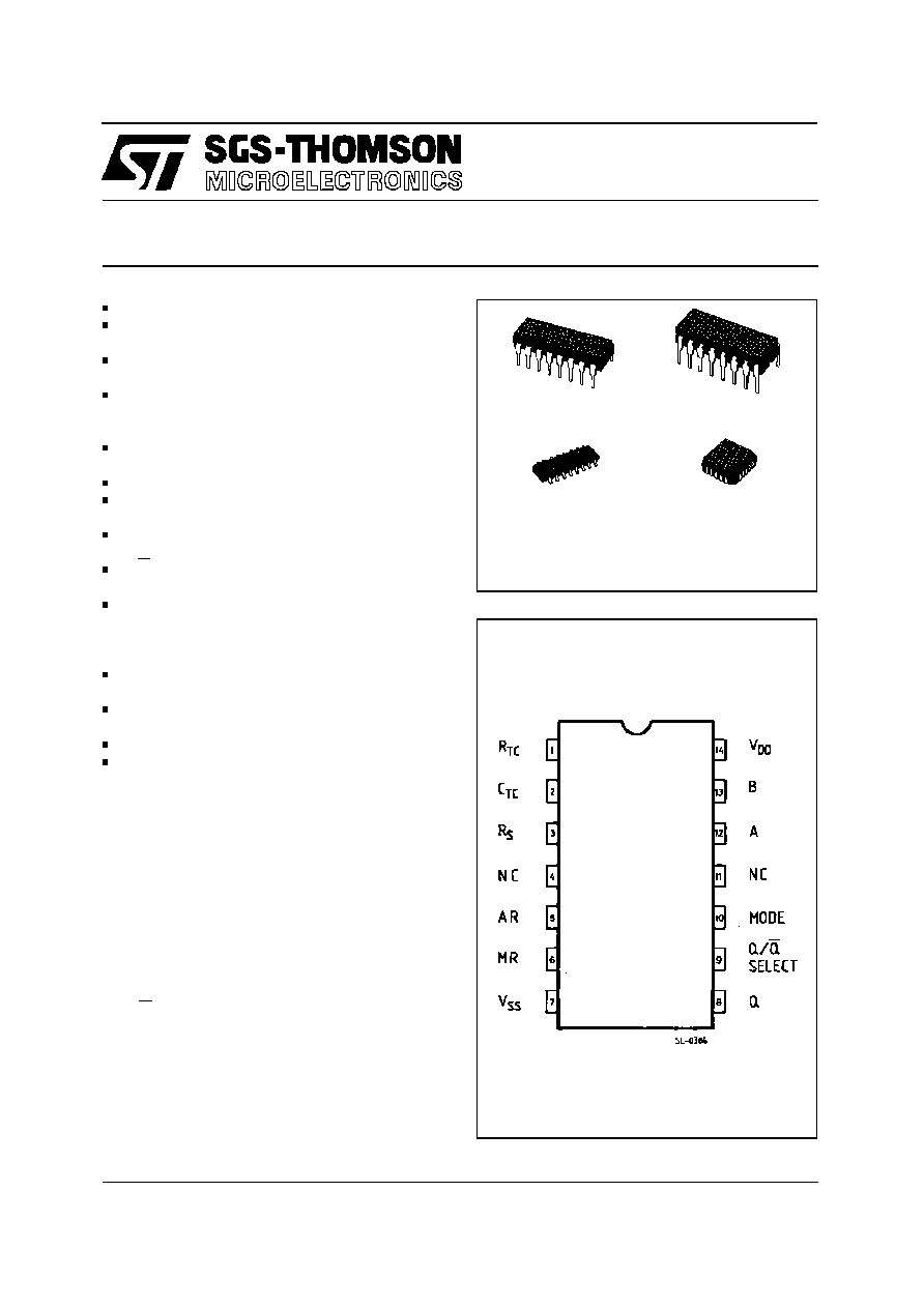
PIN CONNECTION (top view)
The HCC/HCF4541B Programmable Timer is com-
posed of a 16-stage binary counter, an oscillator
controlled by 2 external resistors and a capacitor, an
output control logic and an automatic power-on
reset circuit. The counter varies on positive-edge
clock transation and it can be cleared by the MAS-
TER RESET input. The output from this timer is the
Q or Q output from the 8th, 13th, or 16th counter
stage. The choice of the stage depends on the time-
select inputs A or B (see frequency selection table).
The output is available in one of the two modes that
can be selected via the MODE input, pin 10 (see
truth table). The output turns out as a continuous
square wave, with a frequency equal to the oscillator
frequency divided by 2
N
. When this MODE input is
1/11
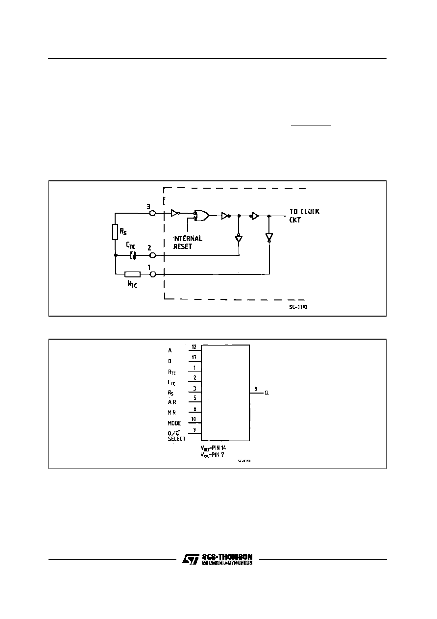
RC Oscillator Circuit.
a logic " 1 ", when it is a logic " 0 " and after a MAS-
TER RESET is started, and Q output has been se-
lected, the output goes up to a high state after 2
N-1
counts. It remains in that state till another MASTER
RESET pulse is apply or the mode input is a logic "
1 ". The process starts by setting the AUTO RESET
input (pin 5) to logic " 0 " and switching power on. If
pin 5 is set to logic " 1 ", the AUTO RESET circuit is
not enabled and counting cannot start till a positive
MASTER RESET pulse is applied, returning to a low
level. The AUTO RESET consumes a remarkable
amount of power and should not be used if low-
power operation is wanted.
The frequency of the oscillator depends on the RC
network. It can be calculated using the following for-
mula:
f
=
1
2.3 R
TC
C
TC
where f is between 1 kHz and 100 kHz
and RS
10 k
and
2 R
TC
FUNCTIONAL DIAGRAM
HCC/HCF4541B
2/11

LOGIC DIAGRAM
RECOMMENDED OPERATING CONDITIONS
Symbol
Parameter
Valu e
Unit
V
DD
Supply Voltage :
HCC Types
HCF Types
3 to 18
3 to 15
V
V
V
I
Input Voltage
0 to V
DD
V
T
op
Operating Temperature : HCC Types
HCF Types
≠ 55 to 125
≠ 40 to 85
∞
C
∞
C
ABSOLUTE MAXIMUM RATINGS
Symbol
Parameter
Valu e
Unit
V
DD
*
Supply Voltage :
HCC Types
HCF Types
≠ 0.5 to + 20
≠ 0.5 to + 18
V
V
V
I
Input Voltage
≠ 0.5 to V
DD
+ 0.5
V
I
I
DC Input Current (any one input)
±
10
mA
P
tot
Total Power Dissipation (per package)
Dissipation per Output Transistor
for T
op
= Full Package-temperature range
200
100
mW
mW
T
op
Operating Temperature : HCC Types
HCF Types
≠ 55 to + 125
≠ 40 to + 85
∞
C
∞
C
T
stg
Storage Temperature
≠ 65 to + 150
∞
C
Stresses above those listed under " Absolute Maximum Ratings " may cause permanent damage to the device. This is a stress
rating only and functional operation of the device at these or any other conditions above those indicated in the operational sec-
tions of this specifi cation is not implied. Exposure to absolute maximum rating conditions for extended periods may affect device
reliability.
* All voltages are with respect to V
SS
(GND).
HCC/HCF4541B
3/11
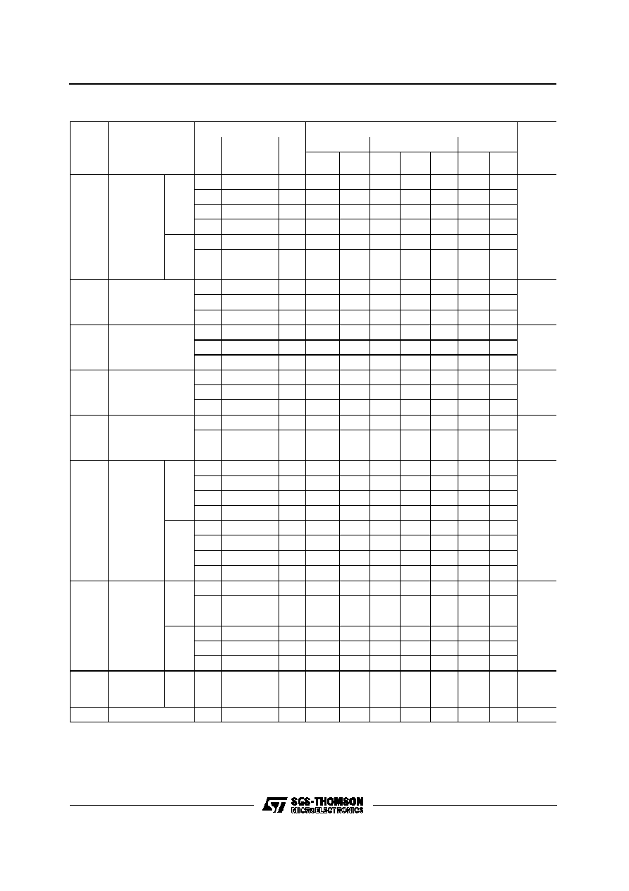
Symbol
Parameter
Test Condi tio ns
Valu e
Unit
V
I
(V)
V
O
(V)
I
O
(uA
)
V
D D
(V)
T
Low
25
∞
C
T
High
Mi n.
Max.
Min.
Typ. Max.
Min. Max.
I
L
Quiescent
Current
HCC
Types
0/5
5
5
0.04
5
150
µ
A
0/10
10
10
0.04
10
300
0/15
15
20
0.04
20
600
0/20
20
100
0.08
100
3000
HCF
Types
0/5
5
5
0.04
5
150
0/10
10
10
0.04
10
300
0/15
15
20
0.04
20
600
V
OH
Output High
Voltage
0/5
< 1
5
4.95
4.95
4.95
V
0/10
< 1
10
9.95
9.95
9.95
0/15
< 1
15
14.95
14.95
14.95
V
OL
Output Low
Voltage
5/0
< 1
5
0.05
0.05
0.05
V
10/0
< 1
10
0.05
0.05
0.05
15/0
< 1
15
0.05
0.05
0.05
V
IH
Input High
Voltage
0.5/4.5 < 1
5
3.5
3.5
3.5
V
1/9
< 1
10
7
7
7
1.5/13.5 < 1
15
11
11
11
V
IL
Input Low
Voltage
4.5/0.5 < 1
5
1.5
1.5
1.5
V
9/1
< 1
10
3
3
3
13.5/1.5 < 1
15
4
4
4
I
OH
Output
Drive
Current
HCC
Types
0/5
4.6
5
≠ 1.9
≠ 1.55 ≠ 3.1
≠ 1.08
mA
0/5
2.5
5
≠ 6.2
≠ 5
≠ 10
≠ 3
0/10
9.5
10
≠ 5.0
≠ 4
≠ 8
≠ 2.8
0/15
13.5
15
≠ 12.6
≠ 10
≠ 20
≠ 7.2
HCF
Types
0/5
4.6
5
≠ 1.85
≠ 1.55 ≠ 3.1
≠ 1.26
0/5
2.5
5
≠ 6.0
≠ 5
≠ 10
≠ 4.1
0/10
9.5
10
≠ 4.8
≠ 4
≠ 8
≠ 3.3
0/15
13.5
15
≠ 12
≠ 10
≠ 20
≠ 8.4
I
OL
Output
Sink
Current
HCC
Types
0/5
0.4
5
1.9
1.55
3.1
1.08
mA
0/10
0.5
10
5.0
4
8
2.8
0/15
1.5
15
12.6
10
20
7.2
HCF
Types
0/5
0.4
5
1.85
1.55
3.1
1.26
0/10
0.5
10
4.8
4
8
3.3
0/15
1.5
15
12
10
20
8.4
I
IH
, I
IL
Input
Leakage
Current
0/18
Any Input
18
±
0.1
±
0.1
≠
5
±
0.1
±
1
µ
A
C
I
Input Capacitance
Any Input
5
7.5
pF
* T
Low
= - 55C for HCC device : - 40C for HCF device.
* T
High
= + 125C for HCC device : + 85C for HCF device.
The Noise Margin for both " 1 " and " 0 " level is : 1V min. with V
DD
= 5V 2V min. with V
DD
= 10V 2.5V min. with V
DD
= 15V
STATIC ELECTRICAL
HCC/HCF4541B
4/11

DYNAMIC ELECTRICAL CHARACTERISTICS (T
amb
= 25
∞
C, C
L
= 50pF, R
L
= 200k
,
typical temperature coefficient for all V
DD
values is 0.3%/
∞
C, all input rise and fall time = 20ns)
Symbol
Parameter
VDD
(V)
Valu es
Unit
Min.
Typ.
Max.
(2
8
)
t
PHL
t
PLH
Propagation Delay Time
Clock to Q
5
3.5
10.5
µ
s
10
1.25
3.8
15
0.9
2.9
(2
16
)
t
PHL
t
PLH
5
6
18
µ
s
10
3.5
10
15
2.5
7.5
t
THL
Transition Time
5
100
200
ns
10
50
100
15
40
80
t
TLH
5
180
360
10
90
180
15
65
130
Master Reset, Clock Pulse Width
5
900
300
ns
10
300
100
15
225
85
f
CL
Maximum Clock Pulse Input Frequency
5
1.5
MHz
10
4
15
6
tr, tf
Maximum Clock Pulse Input Rise or Fall Time
5
Unlimited
µ
s
10
15
HCC/HCF4541B
5/11