 | –≠–ª–µ–∫—Ç—Ä–æ–Ω–Ω—ã–π –∫–æ–º–ø–æ–Ω–µ–Ω—Ç: HD1530JL | –°–∫–∞—á–∞—Ç—å:  PDF PDF  ZIP ZIP |

July 2005
1/5
5
HD1530JL
High Voltage NPN Power Transistor
for High Definition and New Super-Slim CRT Display
Features
STATE-OF-THE-ART TECHNOLOGY:
DIFFUSED COLLECTOR "ENHANCED
GENERATION" EHVS1
WIDER RANGE OF OPTIMUM DRIVE
CONDITIONS
LESS SENSITIVE TO OPERATING
TEMPERATURE VARIATION
Applications
HORIZONTAL DEFLECTION OUTPUT FOR
DIGITAL TV, HDTV, AND HIGH -END
MONITORS
Description
The device uses a Diffused Collector in Planar
technology which adopts "Enhanced High Voltage
Structure" (EHVS1) that was developed to fit
High-Definition CRT displays.
The new HD product series features improved
silicon efficiency, bringing updated performance to
Horizontal Deflection output stages.
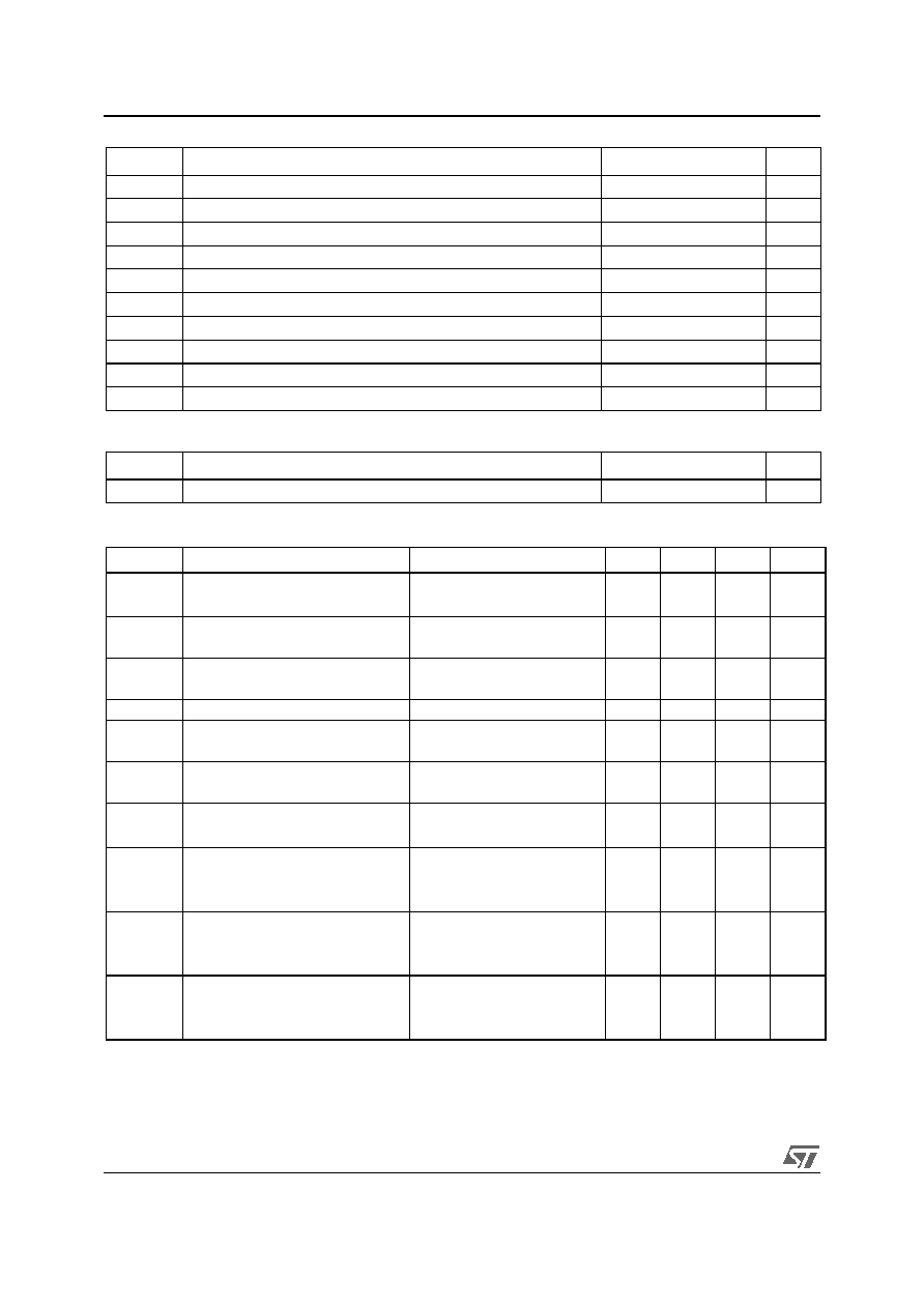
Table 1.
Order Codes
Figure 1.
Package
Figure 2.
Internal Schematic Diagram
TO-264
1
2
3
www.st.com
PRELIMINARY DATA
Part Number
Marking
Package
Packing
HD1530JL
HD1530JL
TO-264
TUBE
rev.1
HD1530JL
2/5
Table 2.
Absolute Maximum Rating
Table 3.
Thermal Data
Table 4.
Electrical Characteristics (T
CASE
= 25∞C; unless otherwise specified)
Note: 1 Pulsed duration = 300
s, duty cycle
1.5%.
Symbol
Parameter
Value
Unit
V
CES
Collector-Emitter Voltage (V
BE
= 0)
1500
V
V
CEO
Collector-Emitter Voltage (I
B
= 0)
700
V
V
EBO
Emitte-Base Voltage (I
C
= 0)
10
V
I
C
Collector Current
26
A
I
CM
Collector Peak Current (t
P
< 5ms)
40
A
I
B
Base Current
10
A
I
BM
Base Peak Current (t
P
< 5ms)
20
A
P
TOT
Total dissipation at T
c
= 25∞C
200
W
T
STG
Storage Temperature
-65 to 150
∞C
T
J
Max. Operating Junction Temperature
150
∞C
Symbol
Parameter
Value
Unit
R
thJC
Thermal Resistance Junction-Case
____________________
Max
0.625
∞C/W
Symbol
Parameter
Test Conditions
Min.
Typ.
Max.
Unit
I
CES
Collector Cut-off Current
(V
BE
= 0)
V
CE
= 1500V
V
CE
= 1500V
____
T
C
= 125∞C
0.2
2
mA
mA
I
EBO
Emitter Cut-off Current
(I
C
= 0)
V
EB
= 5V
10
A
V
CEO(
SUS
)
Note: 1
Collector-Emitter
Susting Voltage (I
B
= 0)
I
C
= 10mA
700
V
V
EBO
Emitter-Base Voltage (I
C
= 0)
I
E
= 10mA
10
V
V
CE(sat)
Note: 1
Collector-Emitter Saturation Voltage I
C
= 13A
_____
I
B
= 3.25A
2.5
V
V
BE(sat)
Note: 1
Base-Emitter Saturation Voltage
I
C
= 13A
_____
I
B
= 3.25A
1
1.5
V
h
FE
DC Current Gain
I
C
= 1A
_____
V
CE
= 5V
I
C
= 13A
____
V
CE
= 5V
5
28
8
t
s
t
f
INDUCTIVE LOAD
Storage Time
Fall Time
I
C
= 12A
____ _
f
h
= 32KHz
I
B(on)
= 1.5A
___
I
B(off)
= -6.1A
3.3
240
s
ns
t
s
t
f
INDUCTIVE LOAD
Storage Time
Fall Time
I
C
= 12A
_____
f
h
= 48KHz
I
B(on)
= 2A
____
I
B(off)
= -6.7A
2.8
200
s
ns
t
s
t
f
INDUCTIVE LOAD
Storage Time
Fall Time
I
C
= 6.5A
_____
f
h
= 100KHz
I
B(on)
= 0.9A
___
I
B(off)
= -4.6A
1.5
110
s
ns

HD1530JL
3/5
Table 5.
TO-264 Mechanical Data
Figure 3.
TO-264 Drawing
HD1530JL
4/5
Table 6.
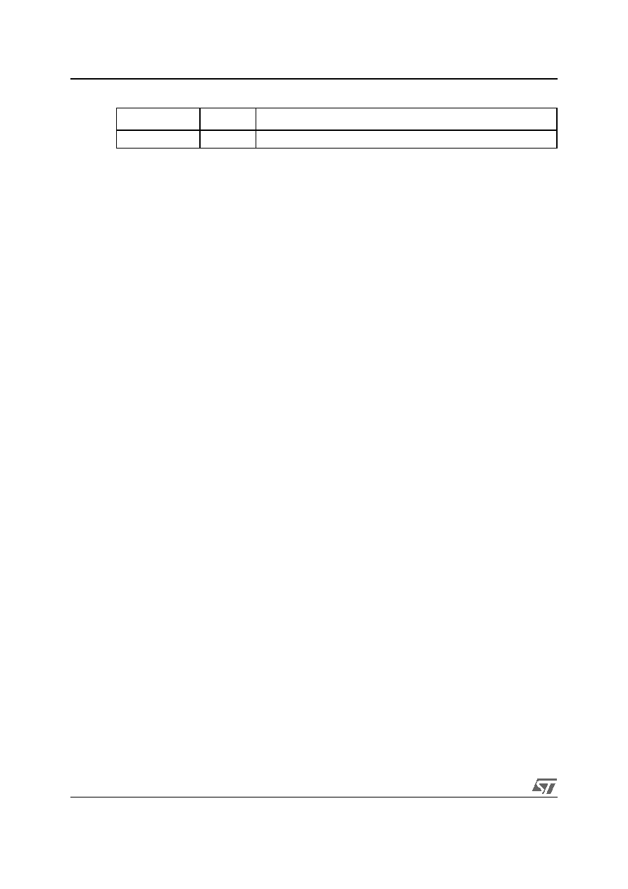
Revision History
Date
Revision
Changes
05-July-2005
1
Initial release.
HD1530JL
5/5
Information furnished is believed to be accurate and reliable. However, STMicroelectronics assumes no responsibility for the consequences
of use of such information nor for any infringement of patents or other rights of third parties which may result from its use. No license is granted
by implication or otherwise under any patent or patent rights of STMicroelectronics. Specifications mentioned in this publication are subject
to change without notice. This publication supersedes and replaces all information previously supplied. STMicroelectronics products are not
authorized for use as critical components in life support devices or systems without express written approval of STMicroelectronics.
The ST logo is a registered trademark of STMicroelectronics.
All other names are the property of their respective owners
© 2005 STMicroelectronics - All rights reserved
STMicroelectronics group of companies
Australia - Belgium - Brazil - Canada - China - Czech Republic - Finland - France - Germany - Hong Kong - India - Israel - Italy - Japan -
Malaysia - Malta - Morocco - Singapore - Spain - Sweden - Switzerland - United Kingdom - United States of America
www.st.com