October 2005
1/10
10
HD1750JL
High Voltage NPN Power Transistor
for High Definition and New Super-Slim CRT Display
Features
STATE-OF-THE-ART TECHNOLOGY:
DIFFUSED COLLECTOR "ENHANCED
GENERATION" EHVS1
WIDER RANGE OF OPTIMUM DRIVE
CONDITIONS
LESS SENSITIVE TO OPERATING
TEMPERATURE VARIATION
Applications
HORIZONTAL DEFLECTION OUTPUT FOR
DIGITAL TV, HDTV AND HIGH -END
MONITORS
Description
The device uses a Diffused Collector in Planar
technology which adopts "Enhanced High Voltage
Structure" (EHVS1) that was developed to fit
High-Definition CRT displays.
The new HD product series features improved
silicon efficiency, bringing updated performance to
Horizontal Deflection output stages.
Order codes
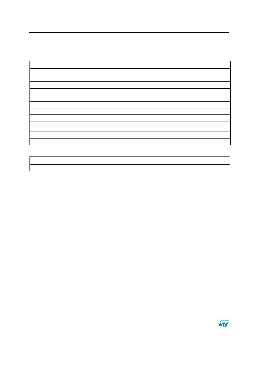
Internal Schematic Diagram
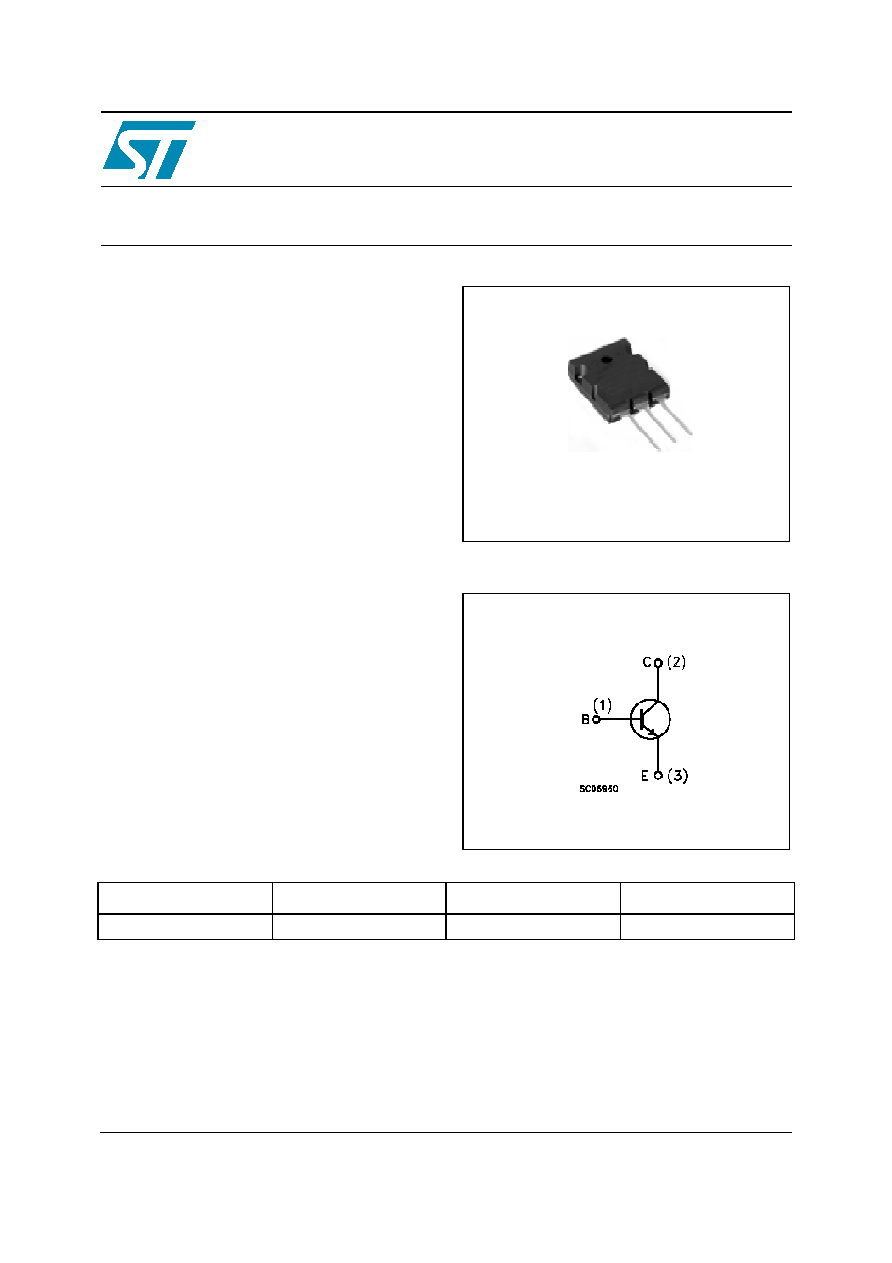
TO-264
1
2
3
www.st.com
PRELIMINARY DATA
Part Number
Marking
Package
Packing
HD1750JL
HD1750JL
TO-264
TUBE
rev.2
1 Electrical ratings
HD1750JL
2/10
1 Electrical
ratings
Table 1.
Absolute Maximum Rating
Table 2.
Thermal Data
Symbol
Parameter
Value
Unit
V
CES
Collector-Emitter Voltage (V
BE
= 0)
1700
V
V
CEO
Collector-Emitter Voltage (I
B
= 0)
800
V
V
EBO
Emitte-Base Voltage (I
C
= 0)
10
V
I
C
Collector Current
24
A
I
CM
Collector Peak Current (t
P
< 5ms)
36
A
I
B
Base Current
12
A
I
BM
Base Peak Current (t
P
< 5ms)
18
A
P
TOT
Total dissipation at T
c
= 25�C
200
W
V
ins
Insulation Withstand Voltage (RMS) from all three Leads to External
Heatsink
2500
V
T
STG
Storage Temperature
-65 to 150
�C
T
J
Max. Operating Junction Temperature
150
�C
Symbol
Parameter
Value
Unit
R
thJC
Thermal Resistance Junction-Case
____________________
Max
0.625
�C/W

HD1750JL
2 Electrical Characteristics
3/10
2 Electrical
Characteristics
(T
CASE
= 25�C; unless otherwise specified)
Table 3.
Electrical Characteristics
Note: 1 Pulsed duration = 300
s, duty cycle
1.5%.
Symbol
Parameter
Test Conditions
Min.
Typ.
Max.
Unit
I
CES
Collector Cut-off Current
(V
BE
= 0)
V
CE
= 1700V
V
CE
= 1700V
___ _
T
C
= 125�C
0.2
2
mA
mA
I
EBO
Emitter Cut-off Current
(I
C
= 0)
V
EB
= 5V
10
A
V
CEO(sus)
Note: 1
Collector-Emitter
Sustaining Voltage (I
B
= 0)
I
C
= 10mA
800
V
V
EBO
Emitter-Base Voltage (I
C
= 0)
I
E
= 10mA
10
V
V
CE(sat)
Note: 1
Collector-Emitter Saturation
Voltage
I
C
= 12A
_____
I
B
= 3A
3
V
V
BE(sat)
Note: 1
Base-Emitter Saturation Voltage
I
C
= 12A
_____
I
B
= 3A
0.95
1.5
V
h
FE
DC Current Gain
I
C
= 1A
_ ____
V
CE
= 5V
I
C
= 12A
___ _
V
CE
= 5V
5.5
30
8.5
t
s
t
f
INDUCTIVE LOAD
Storage Time
Fall Time
I
C
= 12A
___ _ __
f
h
= 31250Hz
I
B(on)
= 1.8A
__ _ _
I
B(off)
= -7.25A
V
CE(fly)
= 1320V
__
V
BE(off)
= -2.7V
L
BB(on)
= 0.8
H
3
300
3.6
450
s
ns
t
s
t
f
INDUCTIVE LOAD
Storage Time
Fall Time
I
C
= 6.5A
__ _ __
f
h
= 100kHz
I
B(on)
= 1.1A
__ _ _
I
B(off)
= -5.25A
V
CE(fly)
= 1220V
__
V
BE(off)
= -2.7V
L
BB(on)
= 0.25
H
1.6
110
2
220
s
ns

HD1750JL
2 Electrical Characteristics
5/10
Figure 7.
Collector-Emitter Saturation Voltage Figure 8.
Base-Emitter Saturation Voltage
Figure 9.
Power Losses
Figure 10. Power Losses
Figure 11. Inductive Load Switching Time
Figure 12. Inductive Load Switching Time
