 | –≠–ª–µ–∫—Ç—Ä–æ–Ω–Ω—ã–π –∫–æ–º–ø–æ–Ω–µ–Ω—Ç: L6451 | –°–∫–∞—á–∞—Ç—å:  PDF PDF  ZIP ZIP |

L6451
28 CHANNEL INK JET DRIVER
ADVANCE DATA
40V DMOS OUTPUT BREAKDOWN
PRECISE OUTPUT ENERGY
ESD OUTPUT PROTECTION WITH CLAMP-
ING DIODES
VERY LOW QUIESCENT CURRENT
PLCC44 OR PQFP44 (10 x 10mm)
DESCRIPTION
The L6451 is realized in Multipower BCD Tech-
nology which combines isolated DMOS power
transistors with CMOS and Bipolar circuits on the
same IC. By using mixed technology it has been
possible to optimize the logic circuitry and the
power stage to achieve the best possible perform-
ances.
Intended to be used in ink jet Printer Applications
as 4 to 28 (2 x 14) lines selectable decoder/driver,
the L6451 device driver has the advantages of
low power CMOS inputs and logic, with 28 high
current and high voltage DMOS outputs capable
of sustaining a maximum of 40V.
On system power up the output drivers are locked
out using the chip enable function; two enable in-
puts are available for the different driver banks.
An internal power-on system is implemented in
order to avoid wrong output commutation during
the supply voltage transients.
Using a mask option during manufacturing allows
a different decoding.
Control of the energy delivered to the print head
is made by means of a special circuitry.
All driver outputs are capable of withstanding a
contact discharge of
±
8kV with the IC biased.
This is advanced information on a new product now in development or undergoing evaluation. Details are subject to change without notice.
May 1995
BLOCK DIAGRAM (case of 4 bit)
PQFP44
PLCC44
MULTIPOWER BCD TECHNOLOGY
1/9

PQFP44 PIN CONNECTION (Top view)
PLCC44 PIN CONNECTION (Top view)
L6451
2/9
PIN FUNCTIONS
Name
Function
V
DD
5V Logic Supply.
GND
Logic and Power Ground.
OUT0 to OUT27
DMOS Outputs.
CLAMP
This pin has to be connected to the power supply voltage of the head resistors. Each of the
output DMOS have their drain connected with the anode of a protection diode, all the cathodes
of the protection diodes are connected to the clamp pin. In order to have the device supplied,
the CLAMP pin needs to be connected to the power..
INA, INB, INC, IND
Decoder inputs.
COM1, COM2
A low logic input on these pins enables the outputs selected by the decoder inputs.
CHIP ENABLE
A logic high enable the chip.
THERMAL DATA
Symbol
Parameter
PQFP44
PLCC44
Unit
R
th j-amb
Thermal Resistance Junction-Ambient
Max.
55 (*)
65 (*)
∞
C/W
(*) device mounted on PCB.
ABSOLUTE MAXIMUM RATINGS
Symbol
Parameter
Value
Unit
V
OUT
Output Voltage
40
V
V
CLAMP
Output Clamping Voltage
40
V
I
OUT
Output Continuous Current
0.8
A
I
PEAK
Output Peak Current (with duty cycle = 10% T
ON
= 4
µ
s)
2
A
T
J
Junction Temperature
150
∞
C
V
DD
Logic Supply Voltage
7
V
V
IN
Input Voltage Range
-0.3V to V
S
+0.3
V
T
amb
Operating Temperature Range
0 to 70
∞
C
T
stg
Storage Temperature Range
-55 to 150
∞
C
L6451
3/9
D.C. ELECTRICAL CHARACTERISTICS at T
amb
= 25
∞
C, V
DD
= 5V, V
clamp
= 18V (unless otherwise specified).
Symbol
Parameter
Test Condition
Min.
Typ.
Max.
Unit
V
DD
Logic Supply Voltage
4.75
5
5.25
V
V
CLAMP
Clamping Voltage
9
38
V
V
IL
Low Level Input Voltage
1.2
V
V
IH
High Level Input Current
V
DD
-1.2
V
I
LL
Low Level Input Current
V
IN
= V
IL
-200
µ
A
I
LH
High Level Input Current
V
IN
= V
IH
10
µ
A
I
DD
Logic Supply Current
(Independent from the output
conditions)
5
mA
V
OUT
Output Saturation Voltage
Tj 25
∞
C D.C. 0.4A
Tj 25
∞
C D.C. 0.5A
Tj 90
∞
C D.C. 0.4A
Tj 90
∞
C D.C. 0.5A
0.9
1.1
1.4
1.7
V
V
V
V
V
CE
Output saturation absolute
voltage variation around the
typ. values for extended
temperature ranges
Tj = 25
∞
C to 90
∞
C D.C.: 0.4A
Tj = 25
∞
C to 90
∞
C D.C.: 0.5A
±
0.2
±
0.25
V
V
R
DS
ON
2.2
A.C. ELECTRICAL CHARACTERISTICS at T
amb
= 25
∞
C, V
DD
= 5V.
Symbol
Signal Name
Parameter
Test Condition
Min.
Typ.
Max.
Unit
T
S
INA, INB, INC,
IND Vs COMn
SET - UP Time
30
ns
T
H
INA, INB, INC,
IND Vs COMn
HOLD Time
0
ns
T
on
COM1,2,3,4
V
S
OUT 0 to N
TURN - ON Time
I
OUT
= 0.5A, R
L
= 39
T
j
= 25 to 90
∞
C
150
ns
T
off
COM1,2,3,4
V
S
OUT 0 to N
TURN - OFF Time
I
OUT
= 0.5A, R
L
= 39
T
j
= 25 to 90
∞
C
150
ns
t
r
Rise Time
100
ns
t
f
Fall Time
100
ns
T
wout
Output Pulse Width
T
win
= 3.5
µ
s R
L
= 40
I
OUT
= 0.5A
- 20
T
win
+ 80
ns
P
D
Maximum allowable
variation of the output
power transmitted by
each driver to the
resistive load
R
L
= 39
V
CLAMP
= 18V
±
4
%
P
D
Maximum
allowable
variation of
the output
power
transmitted
by each
driver to the
resistive load
R
L
= 40
V
clamp
= 18V
Ê4
%
L6451
4/9
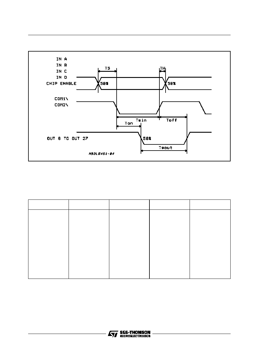
Figure 1: Timing Waveforms
OUTPUT SELECTION
Decoder Truth Table
IND
INC
INB
INA
(LSB)
OUTPUTS
0
0
0
0
0
0
0
0
1
1
1
1
1
1
1
1
0
0
0
0
1
1
1
1
0
0
0
0
1
1
1
1
0
0
1
1
0
0
1
1
0
0
1
1
0
0
1
1
0
1
0
1
0
1
0
1
0
1
0
1
0
1
0
1
0.27
1.26
2.25
3.24
4.23
5.22
6.21
7.20
8.19
9.18
10.17
11.16
12.15
13.14
ALL OFF
ALL OFF
L6451
5/9