 | –≠–ª–µ–∫—Ç—Ä–æ–Ω–Ω—ã–π –∫–æ–º–ø–æ–Ω–µ–Ω—Ç: LM239N | –°–∫–∞—á–∞—Ç—å:  PDF PDF  ZIP ZIP |
1/10
s
WIDE SINGLE SUPPLY VOLTAGE RANGE
OR DUAL SUPPLIES FOR ALL DEVICES :
+2V TO +36V OR ±1V TO ±18V
s
VERY LOW SUPPLY CURRENT (1.1mA)
INDEPENDENT OF SUPPLY VOLTAGE
(1.4mW/comparator at +5V)
s
LOW INPUT BIAS CURRENT : 25nA TYP
s
LOW INPUT OFFSET CURRENT : ±5nA TYP
s
LOW INPUT OFFSET VOLTAGE : ±1mV TYP
s
INPUT COMMON-MODE VOLTAGE RANGE
INCLUDES GROUND
s
LOW OUTPUT SATURATION VOLTAGE :
250mV TYP; (Io = 4mA)
s
DIFFERENTIAL INPUT VOLTAGE RANGE
EQUAL TO THE SUPPLY VOLTAGE
s
TTL, DTL, ECL, MOS, CMOS COMPATIBLE
OUTPUTS
DESCRIPTION
These devices consist of four independent preci-
sion voltage comparators with an offset voltage
specifications as low as 2mV max for LM339A,
LM239A and LM139A. All these comparators
were designed specifically to operate from a sin-
gle power supply aver a wide range of voltages.
Operation from split power supplies is also possi-
ble.
These comparators also have a unique character-
istic in that the input common-mode voltage range
includes ground even though operated from a sin-
gle power supply voltage.
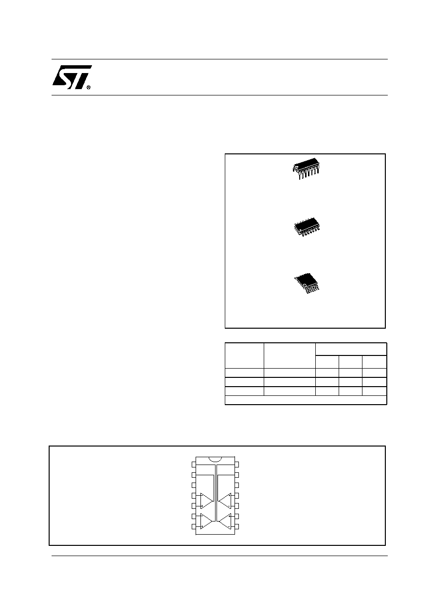
ORDER CODE
N = Dual in Line Package (DIP)
D = Small Outline Package (SO) - also available in Tape & Reel (DT)
P = Thin Shrink Small Outline Package (TSSOP) - only available in Tape
&Reel (PT)
PIN CONNECTIONS (top view)
Part
Number
Temperature
Range
Package
N
D
P
LM139,A
-55∞C, +125∞C
∑
∑
∑
LM239,A
-40∞C, +105∞C
∑
∑
∑
LM339,A
0∞C, +70∞C
∑
∑
∑
Example : LM139AN
N
DIP14
(Plastic Package)
D
SO14
(Plastic Micropackage)
P
TSSOP14
(Thin Shrink Small Outline Package)
4
5
6
7
8
9
10
11
13
1
2
3
14
12
O utput2
O utput4
O utput3
N on-i
nverti
ng i
nput4
V
C C
N on-i
nverti
ng i
nput3
Inverti
ng i
nput4
V
C C
+
O utput1
Inverti
ng i
nput1
N on-i
nverti
ng i
nput2
-
Inverti
ng i
nput3
N on-i
nverti
ng i
nput1
Inverti
ng i
nput2
LM139,A
LM239,A - LM339,A
LOW POWER QUAD VOLTAGE COMPARATORS
March 2003
LM139,A-LM239,A-LM339,A
2/10
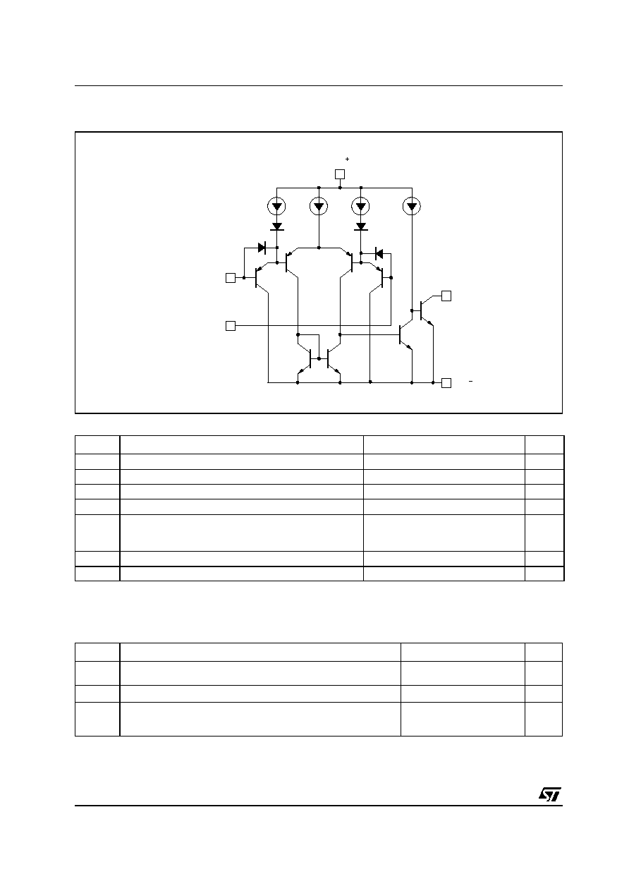
SCHEMATIC DIAGRAM (1/4 LM139)
ABSOLUTE MAXIMUM RATINGS
OPERATING CONDITIONS (T
amb
= 25∞C)
Symbol
Parameter
Value
Unit
V
CC
Supply voltage
±18 or 36
V
V
id
Differential Input Voltage
±36
V
V
i
Input Voltage
-0.3 to +36
V
Output Short-circuit to Ground - note
1)
1.
Short-circuits from the output to V
CC
+
can cause excessive heating and eventual destruction. The maximum output current is approximately 20mA
independent of the magnitude of V
CC
+
.
Infinite
p
d
Power Dissipation
2)
DIP14
SO14
TSSOP14
2.
Pd is calculated with T
amb
= +25∞C, T
j
= +150∞C and R
thja
= 80∞C/W for DIP14 package
= 150∞C/W for SO14 package
= 175∞C/W for TSSOP14 package
1500
830
710
mW
T
stg
Storage Temperature Range
-65 to +150
∞C
T
j
Junction Temperature
+150
∞C
Symbol
Parameter
Value
Unit
V
CC
Supply Voltage
2 to 32
±1 to ±16
V
Vicm
Common Mode Input Voltage Range
0 to (V
CC
+
- 1.5)
V
T
oper
Operating Free-air Temperature Range
LM139, LM139A
LM239, LM239A
LM339, LM339A
-55, +125
-40, +105
0, +70
∞C
Non-inverting
Input
Inverting
Input
3.5
µ
A
CC
V
CC
V
O
V
3.5
µ
A
100
µ
A
100
µ
A
LM139,A-LM239,A-LM339,A
3/10
ELECTRICAL CHARACTERISTICS
V
CC
+
= +5V, V
CC
-
= GND, T
amb
= +25∞C (unless otherwise specified)
Symbol
Parameter
LM139A - LM239A
LM339A
LM139- LM239
LM339
Unit
Min.
Typ.
Max.
Min
Typ.
Max.
V
io
Input Offset Voltage - note
1)
T
amb
= +25∞C
T
min
T
amb
T
max
1.
At output switch point, V
o
1.4V, R
s
= 0 with V
CC
+
from 5V to 30V, and over the full common-mode range (0V to V
CC
+
-1.5V).
1
2
4
1
5
9
mV
I
io
Input Offset Current
T
amb
= +25∞C
T
min
T
amb
T
max
3
25
100
5
50
150
nA
I
ib
Input Bias Current (I
+
or I
-
) - note
2)
T
amb
= +25∞C
T
min
T
amb
T
max
2.
The direction of the input current is out of the IC due to the PNP input stage. This current is essentially constant, independent of the state of the
output, so no loading charge exists on the reference of input lines.
25
100
300
25
250
400
nA
A
vd
Large Signal Voltage Gain
V
CC
= 15V, R
L
= 15k
,
V
o
= 1V to 11V
50
200
50
200
V/mV
I
CC
Supply Current (all comparators)
V
CC
= +5V, no load
V
CC
= +30V, no load
1.1
1.3
2
2.5
1.1
1.3
2
2.5
mA
V
icm
Input Common Mode Voltage Range - note
3)
V
CC
= 30V
T
amb
= +25∞C
T
min
T
amb
T
max
3.
The input common-mode voltage of either input signal voltage should not be allowed to go negative by more than 0.3V. The upper end of the
common-mode voltage range is V
CC
+
-1.5V, but either or both inputs can go to +30V without damage
0
0
V
CC
+
-1.5
V
CC
+
-2
0
0
V
CC
+
-1.5
V
CC
+
-2
V
V
id
Differential Input Voltage -note
4)
4.
The response time specified is for a 100mV input step with 5mV overdrive. For larger overdrive signals 300ns can be obtained
V
CC
+
V
CC
+
V
V
OL
Low Level Output Voltage
V
id
= -1V, I
sink
= 4mA
T
amb
= +25∞C
T
min
T
amb
T
max
250
400
700
250
400
700
mV
I
OH
High Level Output Current (V
id
= 1V)
V
CC
= V
o
= 30V
T
amb
= +25∞C
T
min
T
amb
T
max
0.1
1
0.1
1
nA
µ
A
Isink
Output Sink Currrent
V
id
= 1V, V
o
= 1.5V
6
16
6
16
mA
tre
Response Time - note
5)
R
L
= 5.1k
connected to V
CC
+
5.
Posistive excursions of input voltage may exceed the power supply level. As long as the other voltage remains within the common-mode range, the
comparator will provide a proper output state. The low input voltage state must not be less than -0.3V (or 0.3V bellow the negative power supply, if
used).
1.3
1.3
µ
s
trel
Large Signal Response Time
R
L
= 5.1k
connected to V
CC
+
,
e
l
= TTL,
V
(ref)
= +1.4v
300
300
ns
LM139,A-LM239,A-LM339,A
4/10
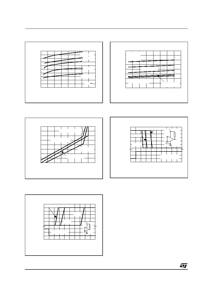
SUPPLY CURRENT versus SUPPLY VOLTAGE
OUTPUT SATURATION VOLTAGE versus
OUTPUT CURRENT
RESPONSE TIME FOR VARIOUS INPUT
OVERDRIVES - POSITIVE TRANSITION
INPUT CURRENT versus SUPPLY VOLTAGE
RESPONSE TIME FOR VAROIOUS INPUT
OVERDRIVES - NEGATIVE TRANSITION
SUPPLY
CURRENT
(mA)
1
0.8
0.6
0.4
0.2
0
10
20
30
40
SUPPLY VOLTAGE (V)
T
amb
= +70∞C
T
amb
= +125∞C
T
amb
= 0∞C
R =
T
amb
= +25∞C
T
amb
= -55∞C
T
amb
= +125∞C
Out of saturation
10
1
10
-3
10
-2
10
-1
10
0
SA
TURATION
VO
LTAGE
(
V)
10
-2
10
-1
10
0
10
1
10
2
OUTPUT SINK CURRENT (mA)
Out of saturation
T
amb
= -55∞C
T
amb
= +25∞C
5V
5.1k
e
o
e
I
6
5
4
3
2
1
0
1
00
50
INPUT
VOL
TAGE
(mV)
OUTPUT
VOLTAG
E
(
V)
0
0.5
1
1.5
2
TIME (
µ
s)
0
p
In ut overdrive : 100mV
T
amb
= +25∞C
5mV
20mV
INPUT
C
URRE
N
T
(
nA
)
20
10
20
30
40
SUPPLY VOLTAGE (V)
T
amb
= +70∞C
T
amb
= +125∞C
T
amb
= -55∞C
40
60
80
0
T
amb
= 0∞C
T
amb
= +25∞C
V = 0V
i
R = 10
i
9
5V
5.1k
e
o
e
I
6
5
4
3
2
0
0
-50
-100
INPUT
V
OLTAGE
(mV)
OUTP
UT
V
O
LTAGE
(
V
)
0
0.5
1
1.5
2
TIME (
µ
s)
Input overdrive : 5mV
20mV
1
100mV
T
amb
= +25∞C
LM139,A-LM239,A-LM339,A
5/10
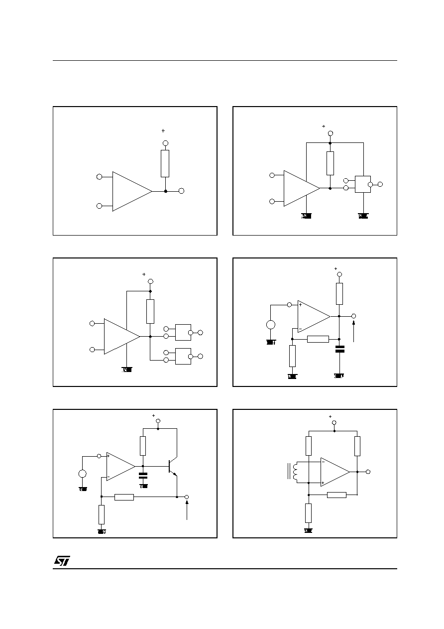
TYPICAL APPICATIONS
BASIC COMPARATOR
DRIVING TTL
LOW FREQUENCY OP AMP
DRIVING CMOS
LOW FREQUENCY OP AMP
TRANSDUCER AMPLIFIER
V
CC
= 5V
15k
V
O
+V
(ref)
-V
(ref)
1/4
LM139
5V
10k
+V
(ref)
-V
(ref)
&
&
1/4
LM139
5V
15k
e
o
0.5
µ
F
100k
e
I
1k
A
= 100
V
~
2N 2222
(e
= 0V for e
= 0V)
I
o
1/4
LM139
5V
100k
+V
(ref)
-V
(ref)
&
1/4
LM139
5V
15k
e
o
0.5
µ
F
100k
e
I
1k
A = 100
V
~
1/4
LM139
5V
10k
eo
20M
3k
Magnetic pick-up
10k
1/4
LM139