Æ
.
WIDE GAIN BANDWIDTH : 1.3MHz
.
INPUT COMMON-MODE VOLTAGE RANGE
INCLUDES GROUND
.
LARGE VOLTAGE GAIN : 100dB
.
VERY LOW SUPPLY CURRENT/AMPLI : 375
µ
A
.
LOW INPUT BIAS CURRENT : 20nA
.
LOW INPUT OFFSET VOLTAGE : 5mV max.
(for more accurate applications, use the equivalent parts
LM124A-LM224A-LM324A which feature 3mV max)
.
LOW INPUT OFFSET CURRENT : 2nA
.
WIDE POWER SUPPLY RANGE :
SINGLE SUPPLY : +3V TO +30V
DUAL SUPPLIES :
±
1.5V TO
±
15V
DESCRIPTION
These circuits consist of four independent, high
gain, internally frequency compensated operational
amplifiers . They operate from a single power supply
over a wide range of voltages. Operation from split
power supplies is also possible and the low power
supply current drain is independent of the magni-
tude of the power supply voltage.
Inve rting Input 2
Non-inve rting Input 2
Non-inve rting Input 1
CC
V
-
CC
V
1
2
3
4
8
5
6
7
9
10
11
12
13
14
+
Output 3
Output 4
Non-inve rting Input 4
Inve rting Input 4
Non-inve rting Input 3
Inve rting Input 3
-
+
-
+
-
+
-
+
Output 1
Inve rting Input 1
Output 2
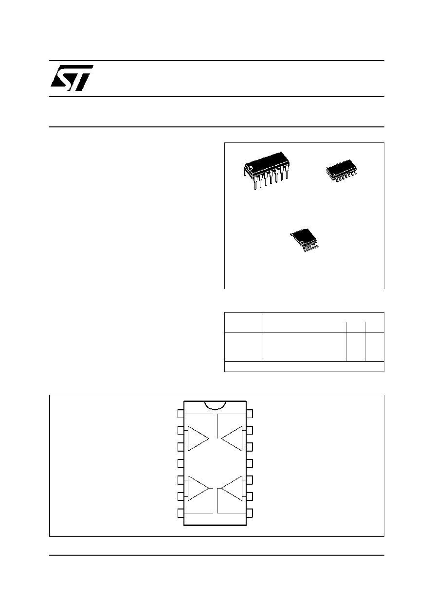
PIN CONNECTIONS (top view)
ORDER CODES
Part
Number
Temperature
Range
Package
N
D
P
LM124
-55
o
C, +125
o
C
∑
∑
∑
LM224
-40
o
C, +105
o
C
∑
∑
∑
LM324
0
o
C, +70
o
C
∑
∑
∑
Example : LM224N
N
DIP14
(Plastic Package)
D
SO14
(Plastic Micropackage)
LOW POWER QUAD OPERATIONAL AMPLIFIERS
LM124
LM224 - LM324
June 1999
P
TSSOP14
(Thin Shrink Small Outline Package)
1/14

ABSOLUTE MAXIMUM RATINGS
Symbol
Parameter
LM124
LM224
LM324
Unit
V
cc
Supply Voltage
±
16 or 32
V
V
i
Input Voltage
-0.3 to +32
V
V
id
Differential Input Voltage - (*)
+32
+32
+32
V
P
tot
Power Dissipation
N Suffix
D Suffix
500
-
500
400
500
400
mW
mW
-
Output Short-circuit Duration - (note 1)
Infinite
I
in
Input Current ≠ (note 6)
50
50
50
mA
T
oper
Operating Free Air Temperature Range
-55 to +125
-40 to +105
0 to +70
o
C
T
stg
Storage Temperature Range
-65 to +150
-65 to +150
-65 to +150
o
C
6
µ
A
4
µ
A
10 0
µ
A
Q2
Q3
Q4
Q1
Inve rting
inpu t
Non-inve rting
inpu t
Q8
Q9
Q10
Q1 1
Q12
5 0
µ
A
Q1 3
Outp ut
Q7
Q6
Q5
R
S C
V
CC
C
C
GND
SCHEMATIC DIAGRAM (1/4 LM124)
LM124 - LM224 - LM324
2/14

ELECTRICAL CHARACTERISTICS
V
CC
+
= +5V, V
CC
≠
= Ground, V
O
= 1.4V, T
amb
= +25
o
C (unless otherwise specified)
Symbol
Parameter
LM124 - LM224 - LM324
Unit
Min.
Typ.
Max.
V
io
Input Offset Voltage (note 3)
T
amb
= +25
o
C
LM324
T
min.
T
amb
T
max
.
LM324
2
5
7
7
9
mV
I
io
Input Offset Current
T
amb
= +25
o
C
T
min.
T
amb
T
max
.
2
30
100
nA
I
ib
Input Bias Current (note 2)
T
amb
= +25
o
C
T
min.
T
amb
T
max
.
20
150
300
nA
A
vd
Large Signal Voltage Gain
(V
CC
+
= +15V, R
L
= 2k
, V
O
= 1.4V to 11.4V)
T
amb
= +25
o
C
T
min.
T
amb
T
max
.
50
25
100
V/mV
SVR
Supply Voltage Rejection Ratio (R
S
10k
)
(V
CC
+
= 5V to 30V)
T
amb
= +25
o
C
T
min.
T
amb
T
max
.
65
65
110
dB
I
CC
Supply Current, all Amp, no load
T
amb
= +25
o
C
V
CC
= +5V
V
CC
= +30V
T
min.
T
amb
T
max
.
V
CC
= +5V
V
CC
= +30V
0.7
1.5
0.8
1.5
1.2
3
1.2
3
mA
V
icm
Input Common Mode Voltage Range
(V
CC
= +30V) - (note 4)
T
amb
= +25
o
C
T
min.
T
amb
T
max.
0
0
V
CC
-1.5
V
CC
-2
V
CMR
Common-mode Rejection Ratio (R
S
10k
)
T
amb
= +25
o
C
T
min.
T
amb
T
max
70
60
80
dB
I
source
Output Current Source (V
id
= +1V)
V
CC
= +15V, V
o
= +2V
20
40
70
mA
I
sink
Output Sink Current (V
id
= -1V)
V
CC
= +15V, V
o
= +2V
V
CC
= +15V, V
o
= +0.2V
10
12
20
50
mA
µ
A
LM124 - LM224 - LM324
3/14

ELECTRICAL CHARACTERISTICS (continued)
Symbol
Parameter
LM124 - LM224 - LM324
Unit
Min.
Typ.
Max.
V
OH
High Level Output Voltage
(V
CC
= +30V)
T
amb
= +25
o
C
R
L
= 2k
T
min
.
T
amb
T
max
.
T
amb
= +25
o
C
R
L
= 10k
T
min
.
T
amb
T
max
.
(V
CC
= +5V, R
L
= 2k
)
T
amb
= +25
o
C
T
min
.
T
amb
T
max
.
26
26
27
27
3.5
3
27
28
V
V
OL
Low Level Output Voltage (R
L
= 10k
)
T
amb
= +25
o
C
T
min
.
T
amb
T
max
.
5
20
20
mV
SR
Slew Rate
V
CC
= 15V, V
I
= 0.5 to 3V, R
L
= 2k
, C
L
= 100pF,
unity gain)
0.4
V/
µ
s
GBP
Gain Bandwidth Product
V
CC
= 30V, f = 100kHz, V
in
= 10mV
R
L
= 2k
, C
L
= 100pF
1.3
MHz
THD
Total Harmonic Distortion
f = 1kHz, A
V
= 20dB, R
L
= 2k
, V
O
= 2V
pp
C
L
= 100pF, V
CC
= 30V
0.015
%
e
n
Equivalent Input Noise Voltage
f = 1kHz, R
s
= 100
, V
CC
= 30V
40
nV
Hz
DV
io
Input Offset Voltage Drift
7
30
µ
V/
o
C
DI
IO
Input Offset Current Drift
10
200
pA/
o
C
V
O
1/V
O
2
Channel Separation (note 5)
1kHz
f
20kHz
120
dB
Notes :
1. Shor t -cir cui t s f rom t he out put t o V
C C
can cause excessi ve heat i ng if V
C C
> 15V. T he maxi mum out put cur rent
is appr oxi mat el y 40mA i ndependent of the magni t ude of V
C C
. D estr ucti ve di ssipat i on can r es ult f r om simul ta-
neous short -cir cuit on al l ampli f iers.
2. The di r ect ion of the i nput cur rent is out of t he IC . Thi s cur r ent is essenti al l y constant, i ndependent of the st ate
of the out put so no l oadi ng change exists on the i nput l i nes.
3. V
o
= 1. 4V , R
s
= 0
,
5V < V
CC
+
< 30V , 0 < V
ic
< V
C C
+
- 1.5V
4. The i nput common- mode vol t age of eit her i nput si gnal volt age shoul d not be allow ed to go negat i ve by mor e
than 0.3V . T he upper end of the common- mode vol tage r ange i s V
C C
+
- 1.5V , but eit her or bot h i nput s can go
to + 32V w i thout damage.
5. Due t o the proxi mit y of ex ternal component s insure t hat coupl ing i s not ori gi nat ing vi a str ay capaci t ance be-
tw een these ext ernal par t s. T hi s t ypi call y can be detect ed as t his t ype of capaci tance i ncreases at higher f re-
quences.
6. This input cur rent onl y exi sts w hen t he volt age at any of t he i nput leads is dr iven negat ive. It i s due t o t he
coll ect or - base juncti on of t he i nput PN P transistor becomi ng forw ar d biased and ther eby act ing as input di-
odes clamps. I n addit i on to thi s di ode act i on, there i s al so N PN par asit i c act ion on the I C chip. t hi s t ransi st or
acti on can cause t he output vol t ages of the Op- amps t o go t o the V
CC
volt age l evel (or to ground f or a l arge
over dri ve) f or t he ti me dur at ion t han an input i s dr iven negati ve.
This i s not destr uct i ve and nor mal out put wi l l set up again f or i nput vol tage higher t han - 0.3V.
LM124 - LM224 - LM324
4/14
