Äîêóìåíòàöèÿ è îïèñàíèÿ www.docs.chipfind.ru
1/55
PRELIMINARY DATA
April 2005
This is preliminary information on a new product now in development or undergoing evaluation. Details are subject to change without notice.
M28W640FCT
M28W640FCB
64 Mbit (4Mb x16, Boot Block)
3V Supply Flash Memory
FEATURES SUMMARY
SUPPLY VOLTAGE
V
DD
= 2.7V to 3.6V Core Power Supply
V
DDQ
= 1.65V to 3.6V for Input/Output
V
PP
= 12V for fast Program (optional)
ACCESS TIME: 70, 85, 90,100ns
PROGRAMMING TIME:
10µs typical
Double Word Programming Option
Quadruple Word Programming Option
COMMON FLASH INTERFACE
MEMORY BLOCKS
Parameter Blocks (Top or Bottom
location)
Main Blocks
BLOCK LOCKING
All blocks locked at Power Up
Any combination of blocks can be locked
WP for Block Lock-Down
SECURITY
128 bit user Programmable OTP cells
64 bit unique device identifier
AUTOMATIC STAND-BY MODE
PROGRAM and ERASE SUSPEND
100,000 PROGRAM/ERASE CYCLES per
BLOCK
ELECTRONIC SIGNATURE
Manufacturer Code: 20h
Top Device Code, M28W640FCT: 8848h
Bottom Device Code, M28W640FCB:
8849h
PACKAGES
Compliant with Lead-Free Soldering
Processes
Lead-Free Versions
Figure 1. Packages
TSOP48 (N)
12 x 20mm
FBGA
TFBGA48 (ZB)
6.39 x 10.5mm

M28W640FCT, M28W640FCB
2/55
TABLE OF CONTENTS
FEATURES SUMMARY . . . . . . . . . . . . . . . . . . . . . . . . . . . . . . . . . . . . . . . . . . . . . . . . . . . . . . . . . . . . . 1
Figure 1. Packages . . . . . . . . . . . . . . . . . . . . . . . . . . . . . . . . . . . . . . . . . . . . . . . . . . . . . . . . . . . . . . 1
SUMMARY DESCRIPTION . . . . . . . . . . . . . . . . . . . . . . . . . . . . . . . . . . . . . . . . . . . . . . . . . . . . . . . . . . . 5
Figure 2. Logic Diagram . . . . . . . . . . . . . . . . . . . . . . . . . . . . . . . . . . . . . . . . . . . . . . . . . . . . . . . . . . 5
Table 1. Signal Names . . . . . . . . . . . . . . . . . . . . . . . . . . . . . . . . . . . . . . . . . . . . . . . . . . . . . . . . . . 5
Figure 3. TSOP Connections . . . . . . . . . . . . . . . . . . . . . . . . . . . . . . . . . . . . . . . . . . . . . . . . . . . . . . 6
Figure 4. TFBGA Connections (Top view through package) . . . . . . . . . . . . . . . . . . . . . . . . . . . . . . 7
Figure 5. Block Addresses . . . . . . . . . . . . . . . . . . . . . . . . . . . . . . . . . . . . . . . . . . . . . . . . . . . . . . . . 8
Figure 6. Protection Register Memory Map . . . . . . . . . . . . . . . . . . . . . . . . . . . . . . . . . . . . . . . . . . . 8
SIGNAL DESCRIPTIONS . . . . . . . . . . . . . . . . . . . . . . . . . . . . . . . . . . . . . . . . . . . . . . . . . . . . . . . . . . . . 9
Address Inputs (A0-A21). . . . . . . . . . . . . . . . . . . . . . . . . . . . . . . . . . . . . . . . . . . . . . . . . . . . . . . . . . 9
Data Input/Output (DQ0-DQ15). . . . . . . . . . . . . . . . . . . . . . . . . . . . . . . . . . . . . . . . . . . . . . . . . . . . . 9
Chip Enable (E). . . . . . . . . . . . . . . . . . . . . . . . . . . . . . . . . . . . . . . . . . . . . . . . . . . . . . . . . . . . . . . . . 9
Output Enable (G). . . . . . . . . . . . . . . . . . . . . . . . . . . . . . . . . . . . . . . . . . . . . . . . . . . . . . . . . . . . . . . 9
Write Enable (W). . . . . . . . . . . . . . . . . . . . . . . . . . . . . . . . . . . . . . . . . . . . . . . . . . . . . . . . . . . . . . . . 9
Write Protect (WP). . . . . . . . . . . . . . . . . . . . . . . . . . . . . . . . . . . . . . . . . . . . . . . . . . . . . . . . . . . . . . . 9
Reset (RP). . . . . . . . . . . . . . . . . . . . . . . . . . . . . . . . . . . . . . . . . . . . . . . . . . . . . . . . . . . . . . . . . . . . . 9
V
DD
Supply Voltage . . . . . . . . . . . . . . . . . . . . . . . . . . . . . . . . . . . . . . . . . . . . . . . . . . . . . . . . . . . . . . 9
V
DDQ
Supply Voltage. . . . . . . . . . . . . . . . . . . . . . . . . . . . . . . . . . . . . . . . . . . . . . . . . . . . . . . . . . . . . 9
V
PP
Program Supply Voltage . . . . . . . . . . . . . . . . . . . . . . . . . . . . . . . . . . . . . . . . . . . . . . . . . . . . . . 9
V
SS
Ground. . . . . . . . . . . . . . . . . . . . . . . . . . . . . . . . . . . . . . . . . . . . . . . . . . . . . . . . . . . . . . . . . . . . 9
BUS OPERATIONS. . . . . . . . . . . . . . . . . . . . . . . . . . . . . . . . . . . . . . . . . . . . . . . . . . . . . . . . . . . . . . . . 10
Read. . . . . . . . . . . . . . . . . . . . . . . . . . . . . . . . . . . . . . . . . . . . . . . . . . . . . . . . . . . . . . . . . . . . . . . . . 10
Write. . . . . . . . . . . . . . . . . . . . . . . . . . . . . . . . . . . . . . . . . . . . . . . . . . . . . . . . . . . . . . . . . . . . . . . . . 10
Output Disable. . . . . . . . . . . . . . . . . . . . . . . . . . . . . . . . . . . . . . . . . . . . . . . . . . . . . . . . . . . . . . . . . 10
Standby. . . . . . . . . . . . . . . . . . . . . . . . . . . . . . . . . . . . . . . . . . . . . . . . . . . . . . . . . . . . . . . . . . . . . . 10
Automatic Standby. . . . . . . . . . . . . . . . . . . . . . . . . . . . . . . . . . . . . . . . . . . . . . . . . . . . . . . . . . . . . . 10
Reset. . . . . . . . . . . . . . . . . . . . . . . . . . . . . . . . . . . . . . . . . . . . . . . . . . . . . . . . . . . . . . . . . . . . . . . . 10
Table 2. Bus Operations . . . . . . . . . . . . . . . . . . . . . . . . . . . . . . . . . . . . . . . . . . . . . . . . . . . . . . . . 10
COMMAND INTERFACE . . . . . . . . . . . . . . . . . . . . . . . . . . . . . . . . . . . . . . . . . . . . . . . . . . . . . . . . . . . 11
Read Memory Array Command . . . . . . . . . . . . . . . . . . . . . . . . . . . . . . . . . . . . . . . . . . . . . . . . . . 11
Read Status Register Command . . . . . . . . . . . . . . . . . . . . . . . . . . . . . . . . . . . . . . . . . . . . . . . . . 11
Read Electronic Signature Command . . . . . . . . . . . . . . . . . . . . . . . . . . . . . . . . . . . . . . . . . . . . . 11
Table 3. Command Codes. . . . . . . . . . . . . . . . . . . . . . . . . . . . . . . . . . . . . . . . . . . . . . . . . . . . . . . 11
Read CFI Query Command . . . . . . . . . . . . . . . . . . . . . . . . . . . . . . . . . . . . . . . . . . . . . . . . . . . . . . 11
Block Erase Command . . . . . . . . . . . . . . . . . . . . . . . . . . . . . . . . . . . . . . . . . . . . . . . . . . . . . . . . . 11
Program Command . . . . . . . . . . . . . . . . . . . . . . . . . . . . . . . . . . . . . . . . . . . . . . . . . . . . . . . . . . . . 12
Double Word Program Command . . . . . . . . . . . . . . . . . . . . . . . . . . . . . . . . . . . . . . . . . . . . . . . . 12
Quadruple Word Program Command . . . . . . . . . . . . . . . . . . . . . . . . . . . . . . . . . . . . . . . . . . . . . 12

3/55
M28W640FCT, M28W640FCB
Clear Status Register Command . . . . . . . . . . . . . . . . . . . . . . . . . . . . . . . . . . . . . . . . . . . . . . . . . 12
Program/Erase Suspend Command . . . . . . . . . . . . . . . . . . . . . . . . . . . . . . . . . . . . . . . . . . . . . . 12
Program/Erase Resume Command . . . . . . . . . . . . . . . . . . . . . . . . . . . . . . . . . . . . . . . . . . . . . . . 13
Protection Register Program Command . . . . . . . . . . . . . . . . . . . . . . . . . . . . . . . . . . . . . . . . . . . 13
Block Lock Command . . . . . . . . . . . . . . . . . . . . . . . . . . . . . . . . . . . . . . . . . . . . . . . . . . . . . . . . . . 13
Block Unlock Command . . . . . . . . . . . . . . . . . . . . . . . . . . . . . . . . . . . . . . . . . . . . . . . . . . . . . . . . 13
Block Lock-Down Command . . . . . . . . . . . . . . . . . . . . . . . . . . . . . . . . . . . . . . . . . . . . . . . . . . . . 13
Table 4. Commands . . . . . . . . . . . . . . . . . . . . . . . . . . . . . . . . . . . . . . . . . . . . . . . . . . . . . . . . . . . 14
Table 5. Read Electronic Signature . . . . . . . . . . . . . . . . . . . . . . . . . . . . . . . . . . . . . . . . . . . . . . . 14
Table 6. Read Block Lock Signature . . . . . . . . . . . . . . . . . . . . . . . . . . . . . . . . . . . . . . . . . . . . . . 15
Table 7. Read Protection Register and Lock Register . . . . . . . . . . . . . . . . . . . . . . . . . . . . . . . . . 15
Table 8. Program, Erase Times and Program/Erase Endurance Cycles
. . . . . . . . . . . . . . . . . . . 16
BLOCK LOCKING. . . . . . . . . . . . . . . . . . . . . . . . . . . . . . . . . . . . . . . . . . . . . . . . . . . . . . . . . . . . . . . . . 17
Reading a Block's Lock Status . . . . . . . . . . . . . . . . . . . . . . . . . . . . . . . . . . . . . . . . . . . . . . . . . . 17
Locked State . . . . . . . . . . . . . . . . . . . . . . . . . . . . . . . . . . . . . . . . . . . . . . . . . . . . . . . . . . . . . . . . . 17
Unlocked State. . . . . . . . . . . . . . . . . . . . . . . . . . . . . . . . . . . . . . . . . . . . . . . . . . . . . . . . . . . . . . . . 17
Lock-Down State . . . . . . . . . . . . . . . . . . . . . . . . . . . . . . . . . . . . . . . . . . . . . . . . . . . . . . . . . . . . . . 17
Locking Operations During Erase Suspend . . . . . . . . . . . . . . . . . . . . . . . . . . . . . . . . . . . . . . . . 17
Table 9. Block Lock Status . . . . . . . . . . . . . . . . . . . . . . . . . . . . . . . . . . . . . . . . . . . . . . . . . . . . . . 18
Table 10. Protection Status . . . . . . . . . . . . . . . . . . . . . . . . . . . . . . . . . . . . . . . . . . . . . . . . . . . . . . 18
STATUS REGISTER . . . . . . . . . . . . . . . . . . . . . . . . . . . . . . . . . . . . . . . . . . . . . . . . . . . . . . . . . . . . . . . 19
Program/Erase Controller Status (Bit 7) . . . . . . . . . . . . . . . . . . . . . . . . . . . . . . . . . . . . . . . . . . . . . 19
Erase Suspend Status (Bit 6) . . . . . . . . . . . . . . . . . . . . . . . . . . . . . . . . . . . . . . . . . . . . . . . . . . . . . 19
Erase Status (Bit 5) . . . . . . . . . . . . . . . . . . . . . . . . . . . . . . . . . . . . . . . . . . . . . . . . . . . . . . . . . . . . . 19
Program Status (Bit 4) . . . . . . . . . . . . . . . . . . . . . . . . . . . . . . . . . . . . . . . . . . . . . . . . . . . . . . . . . . . 19
V
PP
Status (Bit 3). . . . . . . . . . . . . . . . . . . . . . . . . . . . . . . . . . . . . . . . . . . . . . . . . . . . . . . . . . . . . . . 19
Program Suspend Status (Bit 2) . . . . . . . . . . . . . . . . . . . . . . . . . . . . . . . . . . . . . . . . . . . . . . . . . . . 19
Block Protection Status (Bit 1) . . . . . . . . . . . . . . . . . . . . . . . . . . . . . . . . . . . . . . . . . . . . . . . . . . . . . 20
Reserved (Bit 0). . . . . . . . . . . . . . . . . . . . . . . . . . . . . . . . . . . . . . . . . . . . . . . . . . . . . . . . . . . . . . . . 20
Table 11. Status Register Bits . . . . . . . . . . . . . . . . . . . . . . . . . . . . . . . . . . . . . . . . . . . . . . . . . . . . . 20
MAXIMUM RATING. . . . . . . . . . . . . . . . . . . . . . . . . . . . . . . . . . . . . . . . . . . . . . . . . . . . . . . . . . . . . . . . 21
Table 12. Absolute Maximum Ratings . . . . . . . . . . . . . . . . . . . . . . . . . . . . . . . . . . . . . . . . . . . . . . . 21
DC and AC PARAMETERS . . . . . . . . . . . . . . . . . . . . . . . . . . . . . . . . . . . . . . . . . . . . . . . . . . . . . . . . . 22
Table 13. Operating and AC Measurement Conditions . . . . . . . . . . . . . . . . . . . . . . . . . . . . . . . . . . 22
Figure 7. AC Measurement I/O Waveform . . . . . . . . . . . . . . . . . . . . . . . . . . . . . . . . . . . . . . . . . . . 22
Figure 8. AC Measurement Load Circuit. . . . . . . . . . . . . . . . . . . . . . . . . . . . . . . . . . . . . . . . . . . . . 22
Table 14. Capacitance. . . . . . . . . . . . . . . . . . . . . . . . . . . . . . . . . . . . . . . . . . . . . . . . . . . . . . . . . . . 22
Table 15. DC Characteristics . . . . . . . . . . . . . . . . . . . . . . . . . . . . . . . . . . . . . . . . . . . . . . . . . . . . . 23
Figure 9. Read AC Waveforms . . . . . . . . . . . . . . . . . . . . . . . . . . . . . . . . . . . . . . . . . . . . . . . . . . . . 24
Table 16. Read AC Characteristics
. . . . . . . . . . . . . . . . . . . . . . . . . . . . . . . . . . . . . . . . . . . . . . . . . 24
Figure 10.Write AC Waveforms, Write Enable Controlled . . . . . . . . . . . . . . . . . . . . . . . . . . . . . . . . 25
Table 17. Write AC Characteristics, Write Enable Controlled . . . . . . . . . . . . . . . . . . . . . . . . . . . . . 26

M28W640FCT, M28W640FCB
4/55
Figure 11.Write AC Waveforms, Chip Enable Controlled . . . . . . . . . . . . . . . . . . . . . . . . . . . . . . . . 27
Table 18. Write AC Characteristics, Chip Enable Controlled . . . . . . . . . . . . . . . . . . . . . . . . . . . . . 28
Figure 12.Power-Up and Reset AC Waveforms . . . . . . . . . . . . . . . . . . . . . . . . . . . . . . . . . . . . . . . 29
Table 19. Power-Up and Reset AC Characteristics. . . . . . . . . . . . . . . . . . . . . . . . . . . . . . . . . . . . . 29
PACKAGE MECHANICAL . . . . . . . . . . . . . . . . . . . . . . . . . . . . . . . . . . . . . . . . . . . . . . . . . . . . . . . . . . 30
Figure 13.TSOP48 - 48 lead Plastic Thin Small Outline, 12 x 20mm, Package Outline . . . . . . . . . 30
Table 20. TSOP48 - 48 lead Plastic Thin Small Outline, 12 x 20mm, Package Mechanical Data . 30
Figure 14.TFBGA48 6.39x10.5mm - 8x6 ball array, 0.75mm pitch, Bottom View Package Outline 31
Table 21. TFBGA48 6.39x10.5mm - 8x6 ball array, 0.75mm pitch, Package Mechanical Data . . . 31
Figure 15.TFBGA48 Daisy Chain - Package Connections (Top view through package) . . . . . . . . 32
Figure 16.TFBGA48 Daisy Chain - PCB Connections proposal (Top view through package) . . . . 32
PART NUMBERING . . . . . . . . . . . . . . . . . . . . . . . . . . . . . . . . . . . . . . . . . . . . . . . . . . . . . . . . . . . . . . . 33
Table 22. Ordering Information Scheme . . . . . . . . . . . . . . . . . . . . . . . . . . . . . . . . . . . . . . . . . . . . . 33
Table 23. Daisy Chain Ordering Scheme . . . . . . . . . . . . . . . . . . . . . . . . . . . . . . . . . . . . . . . . . . . . 34
APPENDIX A.BLOCK ADDRESS TABLES . . . . . . . . . . . . . . . . . . . . . . . . . . . . . . . . . . . . . . . . . . . . . 35
Table 24. Top Boot Block Addresses, M28W640FCT . . . . . . . . . . . . . . . . . . . . . . . . . . . . . . . . . . . 35
Table 25. Bottom Boot Block Addresses, M28W640FCB . . . . . . . . . . . . . . . . . . . . . . . . . . . . . . . . 37
APPENDIX B.COMMON FLASH INTERFACE (CFI) . . . . . . . . . . . . . . . . . . . . . . . . . . . . . . . . . . . . . . 39
Table 26. Query Structure Overview . . . . . . . . . . . . . . . . . . . . . . . . . . . . . . . . . . . . . . . . . . . . . . . . 39
Table 27. CFI Query Identification String. . . . . . . . . . . . . . . . . . . . . . . . . . . . . . . . . . . . . . . . . . . . . 39
Table 28. CFI Query System Interface Information . . . . . . . . . . . . . . . . . . . . . . . . . . . . . . . . . . . . . 40
Table 29. Device Geometry Definition . . . . . . . . . . . . . . . . . . . . . . . . . . . . . . . . . . . . . . . . . . . . . . 41
Table 30. Primary Algorithm-Specific Extended Query Table . . . . . . . . . . . . . . . . . . . . . . . . . . . . . 42
Table 31. Security Code Area . . . . . . . . . . . . . . . . . . . . . . . . . . . . . . . . . . . . . . . . . . . . . . . . . . . . . 43
APPENDIX C.FLOWCHARTS AND PSEUDO CODES . . . . . . . . . . . . . . . . . . . . . . . . . . . . . . . . . . . . 44
Figure 17.Program Flowchart and Pseudo Code . . . . . . . . . . . . . . . . . . . . . . . . . . . . . . . . . . . . . . 44
Figure 18.Double Word Program Flowchart and Pseudo Code . . . . . . . . . . . . . . . . . . . . . . . . . . . 45
Figure 19.Quadruple Word Program Flowchart and Pseudo Code . . . . . . . . . . . . . . . . . . . . . . . . . 46
Figure 20.Program Suspend & Resume Flowchart and Pseudo Code . . . . . . . . . . . . . . . . . . . . . . 47
Figure 21.Erase Flowchart and Pseudo Code. . . . . . . . . . . . . . . . . . . . . . . . . . . . . . . . . . . . . . . . . 48
Figure 22.Erase Suspend & Resume Flowchart and Pseudo Code . . . . . . . . . . . . . . . . . . . . . . . . 49
Figure 23.Locking Operations Flowchart and Pseudo Code . . . . . . . . . . . . . . . . . . . . . . . . . . . . . . 50
Figure 24.Protection Register Program Flowchart and Pseudo Code. . . . . . . . . . . . . . . . . . . . . . . 51
APPENDIX D.COMMAND INTERFACE AND PROGRAM/ERASE CONTROLLER STATE. . . . . . . . 52
Table 32. Write State Machine Current/Next, sheet 1 of 2. . . . . . . . . . . . . . . . . . . . . . . . . . . . . . . . 52
Table 33. Write State Machine Current/Next, sheet 2 of 2. . . . . . . . . . . . . . . . . . . . . . . . . . . . . . . . 53
REVISION HISTORY . . . . . . . . . . . . . . . . . . . . . . . . . . . . . . . . . . . . . . . . . . . . . . . . . . . . . . . . . . . . . . . 54
Table 34. Document Revision History . . . . . . . . . . . . . . . . . . . . . . . . . . . . . . . . . . . . . . . . . . . . . . . 54
5/55
M28W640FCT, M28W640FCB
SUMMARY DESCRIPTION
The M28W640FCT and M28W640FCB are 64
Mbit (4 Mbit x 16) non-volatile Flash memories that
can be erased electrically at block level and pro-
grammed in-system on a Word-by-Word basis us-
ing a 2.7V to 3.6V V
DD
supply for the circuitry and
a 1.65V to 3.6V V
DDQ
supply for the Input/Output
pins. An optional 12V V
PP
power supply is provid-
ed to speed up customer programming.
The devices feature an asymmetrical blocked ar-
chitecture. They have an array of 135 blocks: 8
Parameter Blocks of 4 KWord and 127 Main
Blocks of 32 KWord. The M28W640FCT has the
Parameter Blocks at the top of the memory ad-
dress space while the M28W640FCB locates the
Parameter Blocks starting from the bottom. The
memory maps are shown in
Figure 5., Block Ad-
dresses
.
The M28W640FCT and M28W640FCB feature an
instant, individual block locking scheme that al-
lows any block to be locked or unlocked with no la-
tency, enabling instant code and data protection.
All blocks have three levels of protection. They can
be locked and locked-down individually preventing
any accidental programming or erasure. There is
an additional hardware protection against program
and erase. When V
PP
V
PPLK
all blocks are pro-
tected against program or erase. All blocks are
locked at Power Up.
Each block can be erased separately. Erase can
be suspended in order to perform either read or
program in any other block and then resumed.
Program can be suspended to read data in any
other block and then resumed. Each block can be
programmed and erased over 100,000 cycles.
The device includes a 192 bit Protection Register
to increase the protection of a system design. The
Protection Register is divided into a 64 bit segment
and a 128 bit segment. The 64 bit segment con-
tains a unique device number written by ST, while
the second one is one-time-programmable by the
user. The user programmable segment can be
permanently protected.
Figure 6.
, shows the Pro-
tection Register Memory Map.
Program and Erase commands are written to the
Command Interface of the memory. An on-chip
Program/Erase Controller takes care of the tim-
ings necessary for program and erase operations.
The end of a program or erase operation can be
detected and any error conditions identified. The
command set required to control the memory is
consistent with JEDEC standards.
The memory is offered in TSOP48 (12 X 20mm)
and TFBGA48 (6.39 x 10.5mm, 0.75mm pitch)
packages and is supplied with all the bits erased
(set to '1').
In addition to the standard version, the packages
are also available in Lead-free version, in compli-
ance with JEDEC Std J-STD-020B, the ST ECO-
PACK 7191395 Specification, and the RoHS
(Restriction of Hazardous Substances) directive.
All packages are compliant with Lead-free solder-
ing processes.
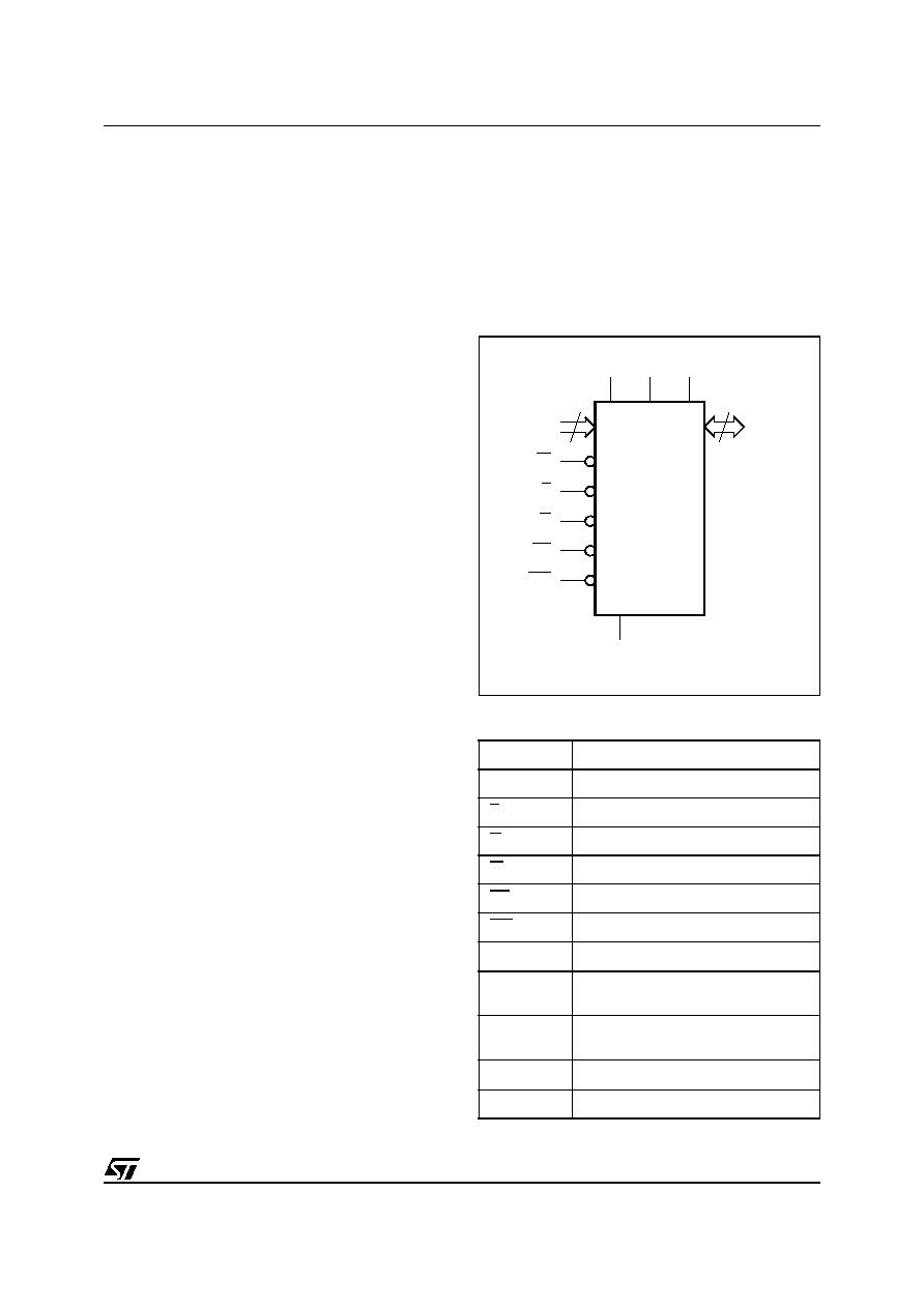
Figure 2. Logic Diagram
Table 1. Signal Names
A0-A21
Address Inputs
DQ0-DQ15
Data Input/Output
E
Chip Enable
G
Output Enable
W
Write Enable
RP
Reset
WP
Write Protect
V
DD
Core Power Supply
V
DDQ
Power Supply for
Input/Output
V
PP
Optional Supply Voltage for
Fast Program & Erase
V
SS
Ground
NC
Not Connected Internally
AI09903
22
A0-A21
W
DQ0-DQ15
VDD
M28W640FCT
M28W640FCB
E
VSS
16
G
RP
WP
VDDQ VPP
Document Outline