
M48T02
M48T12
16 Kbit (2Kb x8) TIMEKEEPER
Æ
SRAM
November 1998
1/15
INTEGRATED ULTRA LOW POWER SRAM,
REAL TIME CLOCK and POWER-FAIL
CONTROL CIRCUIT
BYTEWIDE
TM
RAM-LIKE CLOCK ACCESS
BCD CODED YEAR, MONTH, DAY, DATE,
HOURS, MINUTES and SECONDS
TYPICAL CLOCK ACCURACY of
±
1 MINUTE
a MONTH, AT 25
∞
C
SOFTWARE CONTROLLED CLOCK
CALIBRATION for HIGH ACCURACY
APPLICATIONS
AUTOMATIC POWER-FAILCHIP DESELECTand
WRITE PROTECTION
WRITE PROTECT VOLTAGES
(V
PFD
= Power-fail Deselect Voltage):
≠ M48T02: 4.5V
V
PFD
4.75V
≠ M48T12: 4.2V
V
PFD
4.5V
SELF-CONTAINED BATTERY and CRYSTAL
in the CAPHAT DIP PACKAGE
PIN and FUNCTION COMPATIBLE with
JEDEC STANDARD 2Kb x8 SRAMs
DESCRIPTION
The M48T02/12 TIMEKEEPER
Æ
RAM is a 2Kb x8
non-volatile static RAM and real time clock which
is pin and functional compatible with the DS1642.
A special 24 pin 600mil DIP CAPHAT
TM
package
houses the M48T02/12 silicon with a quartz crystal
and a long life lithium button cell to form a highly
integratedbatterybacked-upmemory and real time
clock solution.
AI01027
11
A0-A10
W
DQ0-DQ7
VCC
M48T02
M48T12
G
VSS
8
E
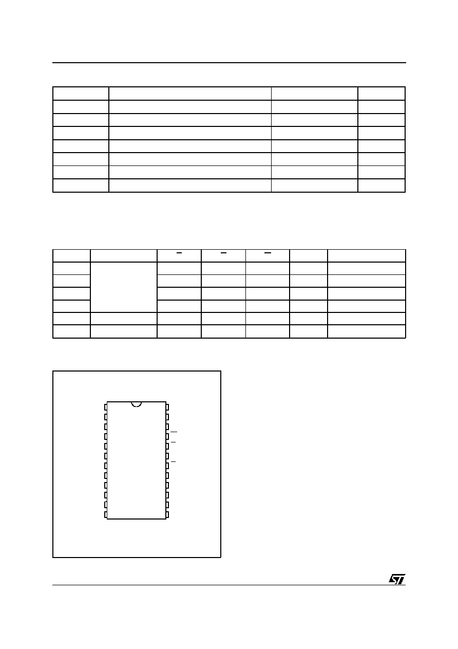
Figure 1. Logic Diagram
A0-A10
Address Inputs
DQ0-DQ7
Data Inputs / Outputs
E
Chip Enable
G
Output Enable
W
Write Enable
V
CC
Supply Voltage
V
SS
Ground
Table 1. Signal Names
24
1
PCDIP24 (PC)
Battery/Crystal CAPHAT
Symbol
Parameter
Value
Unit
T
A
Ambient Operating Temperature
0 to 70
∞
C
T
STG
Storage Temperature (V
CC
Off, Oscillator Off)
≠40 to 85
∞
C
T
SLD
(2)
Lead Solder Temperature for 10 seconds
260
∞
C
V
IO
Input or Output Voltages
≠0.3 to 7
V
V
CC
Supply Voltage
≠0.3 to 7
V
I
O
Output Current
20
mA
P
D
Power Dissipation
1
W
Notes: 1. Stresses greater than those listed under "Absolute Maximum Ratings" may cause permanent damage to the device. This is a
stress rating only and functional operation of the device at these or any other conditions above those indicated in the operational
section of this specification is not implied. Exposure to the absolute maximum rating conditions for extended periods of time may
affect reliability.
2. Soldering temperature not to exceed 260
∞
C for 10 seconds (total thermal budget not to exceed 150
∞
C for longer than 30 seconds).
CAUTION: Negative undershoots below ≠0.3 volts are not allowed on any pin while in the Battery Back-up mode.
Table 2. Absolute Maximum Ratings
(1)
Mode
V
CC
E
G
W
DQ0-DQ7
Power
Deselect
4.75V to 5.5V
or
4.5V to 5.5V
V
IH
X
X
High Z
Standby
Write
V
IL
X
V
IL
D
IN
Active
Read
V
IL
V
IL
V
IH
D
OUT
Active
Read
V
IL
V
IH
V
IH
High Z
Active
Deselect
V
SO
to V
PFD
(min)
X
X
X
High Z
CMOS Standby
Deselect
V
SO
X
X
X
High Z
Battery Back-up Mode
Notes: X = V
IH
or V
IL
; V
SO
= Battery Back-up Switchover Voltage.
Table 3. Operating Modes
A1
A0
DQ0
A7
A4
A3
A2
A6
A5
A10
A8
A9
DQ7
W
G
E
DQ5
DQ1
DQ2
DQ3
VSS
DQ4
DQ6
VCC
AI01028
M48T02
M48T12
8
1
2
3
4
5
6
7
9
10
11
12
16
15
24
23
22
21
20
19
18
17
14
13
Figure 2. DIP Pin Connections
The M48T02/12 button cell has sufficient capacity
and storagelife to maintain data and clockfunction-
ality for an accumulated time period of at least 10
years in the absence of power over the operating
temperature range.
The M48T02/12 is a non-volatile pin and function
equivalent to any JEDEC standard 2Kb x8 SRAM.
It also easily fits into many ROM, EPROM, and
EEPROM sockets, providing the non-volatility of
PROMs without any requirement for special write
timing or limitations on the number of writes that
can be performed.
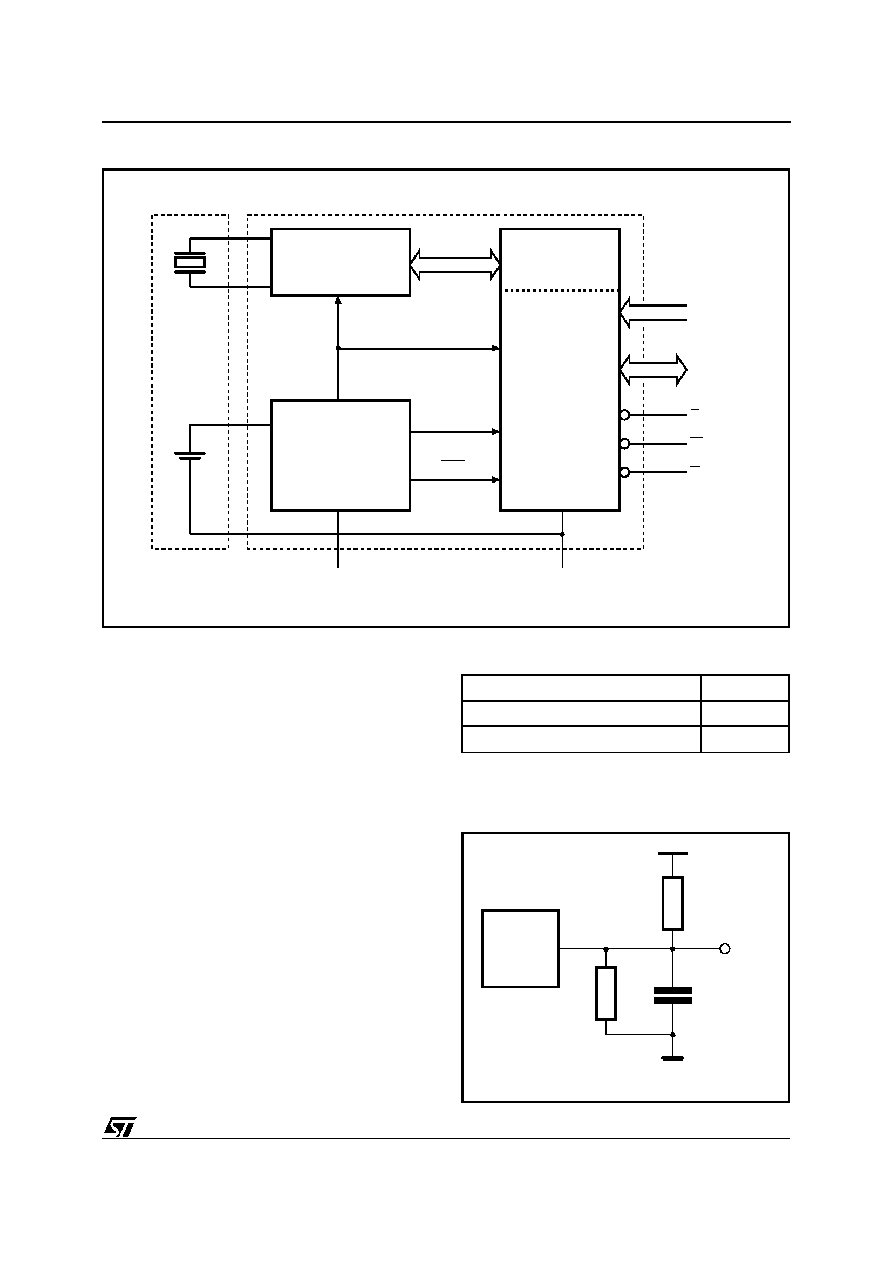
As Figure 3 shows, the staticmemory array and the
quartz controlled clock oscillator of the M48T02/12
are integrated on one silicon chip. The two circuits
are interconnected at the upper eight memory lo-
cations to provide user accessible BYTEWIDE
clock information in the bytes with addresses7F8h-
7FFh. The clock locations contain the year, month,
date, day, hour, minute, and secondin 24 hour BCD
format. Corrections for 28, 29 (leap year), 30, and
31 day months are made automatically.
DESCRIPTION (cont'd)
2/15
M48T02, M48T12
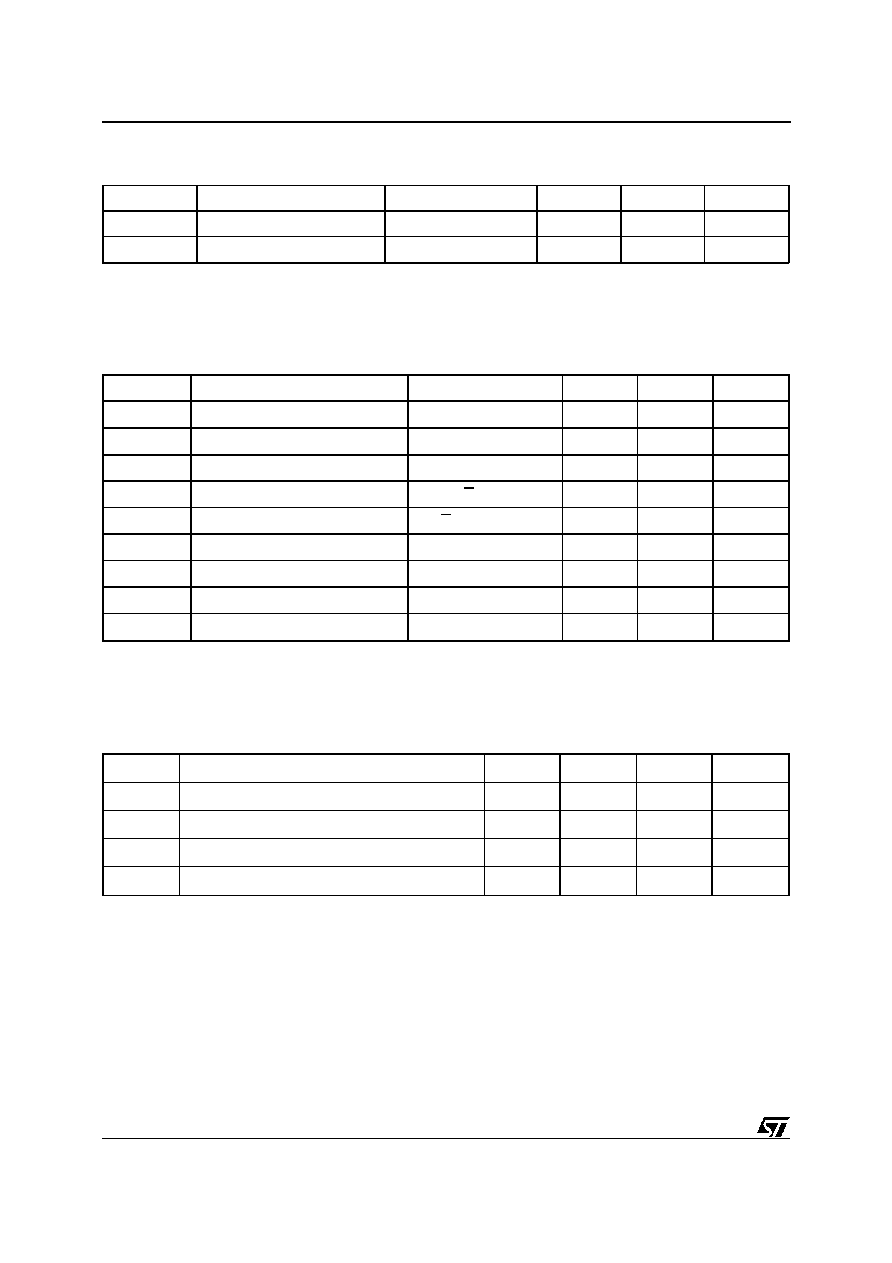
AI01019
5V
OUT
CL = 100pF
CL includes JIG capacitance
1.8k
DEVICE
UNDER
TEST
1k
Figure 4. AC Testing Load Circuit
Input Rise and Fall Times
5ns
Input Pulse Voltages
0V to 3V
Input and Output Timing Ref. Voltages
1.5V
Note that Output Hi-Z is defined as the point where data is no
longer driven.
Table 4. AC Measurement Conditions
AI01329
LITHIUM
CELL
OSCILLATOR AND
CLOCK CHAIN
VPFD
VCC
VSS
32,768 Hz
CRYSTAL
VOLTAGE SENSE
AND
SWITCHING
CIRCUITRY
8 x 8 BiPORT
SRAM ARRAY
2040 x 8
SRAM ARRAY
A0-A10
DQ0-DQ7
E
W
G
POWER
BOK
Figure 3. Block Diagram
Byte 7F8h is the clock control register. This byte
controls user access to the clock information and
also stores the clock calibration setting.
The eight clock bytes are not the actual clock
counters themselves; they are memory locations
consisting of BiPORT
TM
read/write memory cells.
The M48T02/12 includes a clock control circuit
which updates the clock bytes with current informa-
tion once per second. The information can be
accessed by the user in the same manner as any
other location in the static memory array.
The M48T02/12 also has its own Power-fail Detect
circuit. The control circuitry constantlymonitors the
single 5V supply for an out of tolerance condition.
When V
CC
is out of tolerance, the circuit write
protects the SRAM, providing a high degree of data
security in the midst of unpredictable system op-
eration brought on by low V
CC
. As V
CC
falls below
approximately3V, the control circuitry connectsthe
battery which maintains data and clock operation
until valid power returns.
3/15
M48T02, M48T12
Symbol
Parameter
Test Condition
Min
Max
Unit
I
LI
(1)
Input Leakage Current
0V
V
IN
V
CC
±
1
µ
A
I
LO
(1)
Output Leakage Current
0V
V
OUT
V
CC
±
5
µ
A
I
CC
Supply Current
Outputs open
80
mA
I
CC1
(2)
Supply Current (Standby) TTL
E = V
IH
3
mA
I
CC2
(2)
Supply Current (Standby) CMOS
E = V
CC
≠ 0.2V
3
mA
V
IL
(3)
Input Low Voltage
≠0.3
0.8
V
V
IH
Input High Voltage
2.2
V
CC
+ 0.3
V
V
OL
Output Low Voltage
I
OL
= 2.1mA
0.4
V
V
OH
Output High Voltage
I
OH
= ≠1mA
2.4
V
Notes: 1. Outputs Deselected.
2. Measured with Control Bits set as follows: R = '1'; W, ST, KS, FT = '0'.
Table 6. DC Characteristics
(T
A
= 0 to 70
∞
C; V
CC
= 4.75V to 5.5V or 4.5V to 5.5V)
Symbol
Parameter
Test Condition
Min
Max
Unit
C
IN
Input Capacitance
V
IN
= 0V
10
pF
C
IO
(2)
Input / Output Capacitance
V
OUT
= 0V
10
pF
Notes: 1. Effective capacitance measured with power supply at 5V.
2. Outputs deselected.
Table 5. Capacitance
(1)
(T
A
= 25
∞
C, f = 1 MHz )
Symbol
Parameter
Min
Typ
Max
Unit
V
PFD
Power-fail Deselect Voltage (M48T02)
4.5
4.6
4.75
V
V
PFD
Power-fail Deselect Voltage (M48T12)
4.2
4.3
4.5
V
V
SO
Battery Back-up Switchover Voltage
3.0
V
t
DR
(2)
Expected Data Retention Time
10
YEARS
Notes: 1. All voltages referenced to V
SS
.
2. At 25
∞
C.
Table 7. Power Down/Up Trip Points DC Characteristics
(1)
(T
A
= 0 to 70
∞
C)
4/15
M48T02, M48T12

Symbol
Parameter
Min
Max
Unit
t
PD
E or W at V
IH
before Power Down
0
µ
s
t
F
(1)
V
PFD
(max) to V
PFD
(min) V
CC
Fall Time
300
µ
s
t
FB
(2)
V
PFD
(min) to V
SO
V
CC
Fall Time
10
µ
s
t
R
V
PFD
(min) to V
PFD
(max) V
CC
Rise Time
0
µ
s
t
RB
V
SO
to V
PFD
(min) V
CC
Rise Time
1
µ
s
t
REC
E or W at V
IH
after Power Up
2
ms
Notes: 1. V
PFD
(max) to V
PFD
(min) fall time of less than t
F
may result in deselection/write protection not occurring until 50
µ
s after
V
CC
passes V
PFD
(min).
2. V
PFD
(min) to V
SO
fall time of less than t
FB
may cause corruption of RAM data.
Table 8. Power Down/Up Mode AC Characteristics
(T
A
= 0 to 70
∞
C)
AI00606
VCC
INPUTS
(PER CONTROL INPUT)
OUTPUTS
DON'T CARE
HIGH-Z
tF
tFB
tR
tREC
tPD
tRB
tDR
VALID
VALID
NOTE
(PER CONTROL INPUT)
RECOGNIZED
RECOGNIZED
VPFD (max)
VPFD (min)
VSO
Figure 5. Power Down/Up Mode AC Waveforms
Note: Inputs may or may not be recognized at this time. Caution should be taken to keep E high as V
CC
rises past V
PFD
(min). Some systems
may perform inadvertent write cycles after V
CC
rises above V
PFD
(min) but before normal system operations begin. Even though a power on
reset is being applied to the processor, a reset condition may not occur until after the system clock is running.
5/15
M48T02, M48T12