1/19
May 2000
M48T35AY
M48T35AV
256 Kbit (32Kb x8) TIMEKEEPER
Æ
SRAM
s
INTEGRATED ULTRA LOW POWER SRAM,
REAL TIME CLOCK, POWER-FAIL CONTROL
CIRCUIT and BATTERY
s
BYTEWIDETM RAM-LIKE CLOCK ACCESS
s
BCD CODED YEAR, MONTH, DAY, DATE,
HOURS, MINUTES and SECONDS
s
BATTERY LOW FLAG (BOK)
s
FREQUENCY TEST OUTPUT for REAL TIME
CLOCK
s
AUTOMATIC POWER-FAIL CHIP DESELECT
and WRITE PROTECTION
s
WRITE PROTECT VOLTAGES
(V
PFD
= Power-fail Deselect Voltage):
≠ M48T35AY: 4.2V
V
PFD
4.5V
≠ M48T35AV: 2.7V
V
PFD
3.0V
s
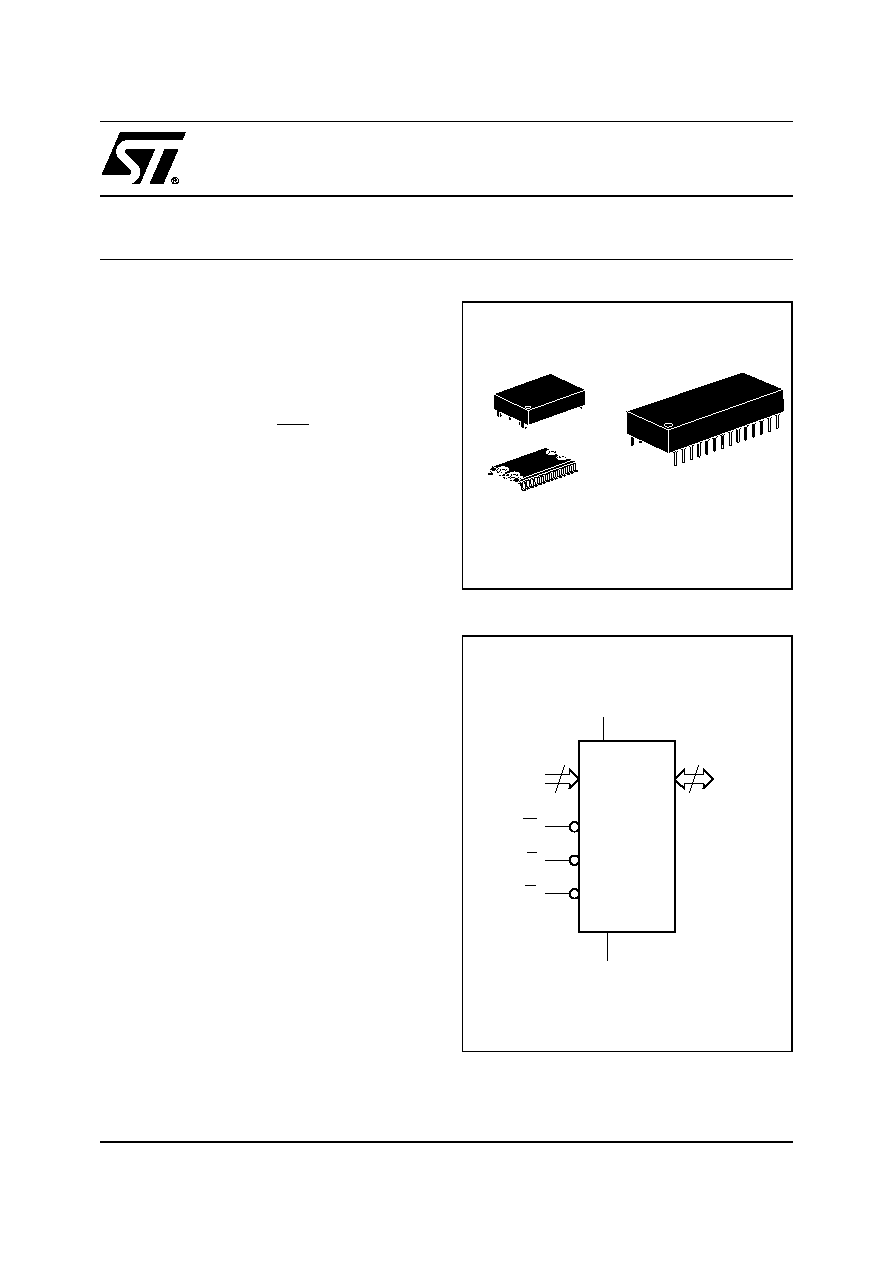
SELF-CONTAINED BATTERY and CRYSTAL
in the CAPHAT DIP PACKAGE
s
SOIC PACKAGE PROVIDES DIRECT
CONNECTION for a SNAPHAT HOUSING
CONTAINING the BATTERY and CRYSTAL
s
SNAPHAT
Æ
HOUSING (BATTERY and
CRYSTAL) is REPLACEABLE
s
PIN and FUNCTION COMPATIBLE with
JEDEC STANDARD 32Kb x8 SRAMs
DESCRIPTION
The M48T35AY/35AV TIMEKEEPER
Æ
RAM is a
32Kb x8 non-volatile static RAM and real time
clock. The monolithic chip is available in two spe-
cial packages to provide a highly integrated bat-
tery backed-up memory and real time clock
solution.
The M48T35AY/35AV is a non-volatile pin and
function equivalent to any JEDEC standard 32Kb
x8 SRAM. It also easily fits into many ROM,
EPROM, and EEPROM sockets, providing the
non-volatility of PROMs without any requirement
for special write timing or limitations on the number
of writes that can be performed.
Figure 1. Logic Diagram
AI02797B
15
A0-A14
W
DQ0-DQ7
VCC
M48T35AY
M48T35AV
G
VSS
8
E
28
1
28
1
SOH28 (MH)
SNAPHAT (SH)
Battery/Crystal
PCDIP28 (PC)
Battery/Crystal
CAPHAT
M48T35AY, M48T35AV
2/19
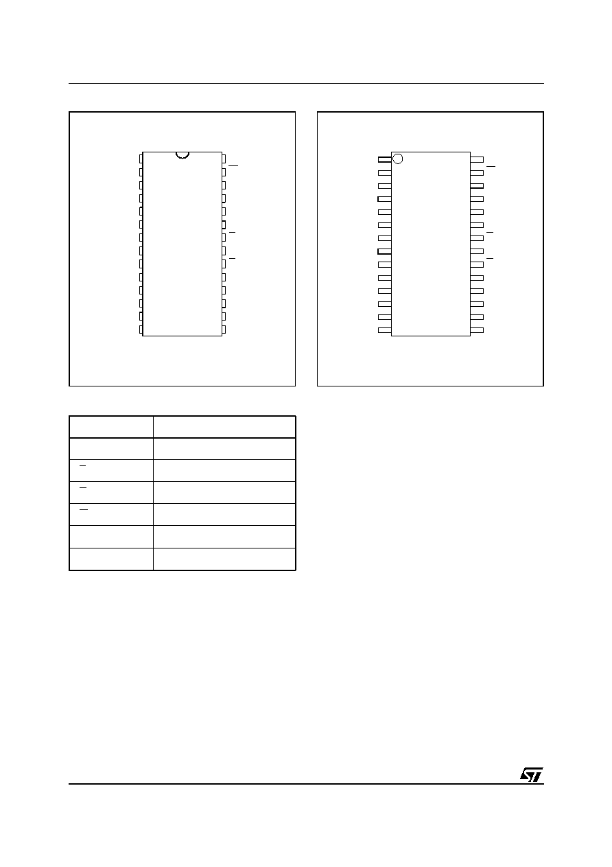
Figure 2A. DIP Connections
A1
A0
DQ0
A7
A4
A3
A2
A6
A5
A13
A10
A8
A9
DQ7
W
A11
G
E
DQ5
DQ1
DQ2
DQ3
VSS
DQ4
DQ6
A12
A14
VCC
AI02798B
8
1
2
3
4
5
6
7
9
10
11
12
13
14
16
15
28
27
26
25
24
23
22
21
20
19
18
17
M48T35AY
M48T35AV
Figure 2B. SOIC Connections
AI02799
8
2
3
4
5
6
7
9
10
11
12
13
14
22
21
20
19
18
17
16
15
28
27
26
25
24
23
1
A1
A0
DQ0
A7
A4
A3
A2
A6
A5
A13
A10
A8
A9
DQ7
W
A11
G
E
DQ5
DQ1
DQ2
DQ3
VSS
DQ4
DQ6
A12
A14
VCC
M48T35AY
M48T35AV
completion of the surface mount process. Inser-
tion of the SNAPHAT housing after reflow pre-
vents potential battery and crystal damage due to
the high temperatures required for device surface-
mounting. The SNAPHAT housing is keyed to pre-
vent reverse insertion.
The SOIC and battery/crystal packages are
shipped separately in plastic anti-static tubes or in
Tape & Reel form.
For the 28 lead SOIC, the battery/crystal package
(i.e. SNAPHAT) part number is "M4T28-
BR12SH1".
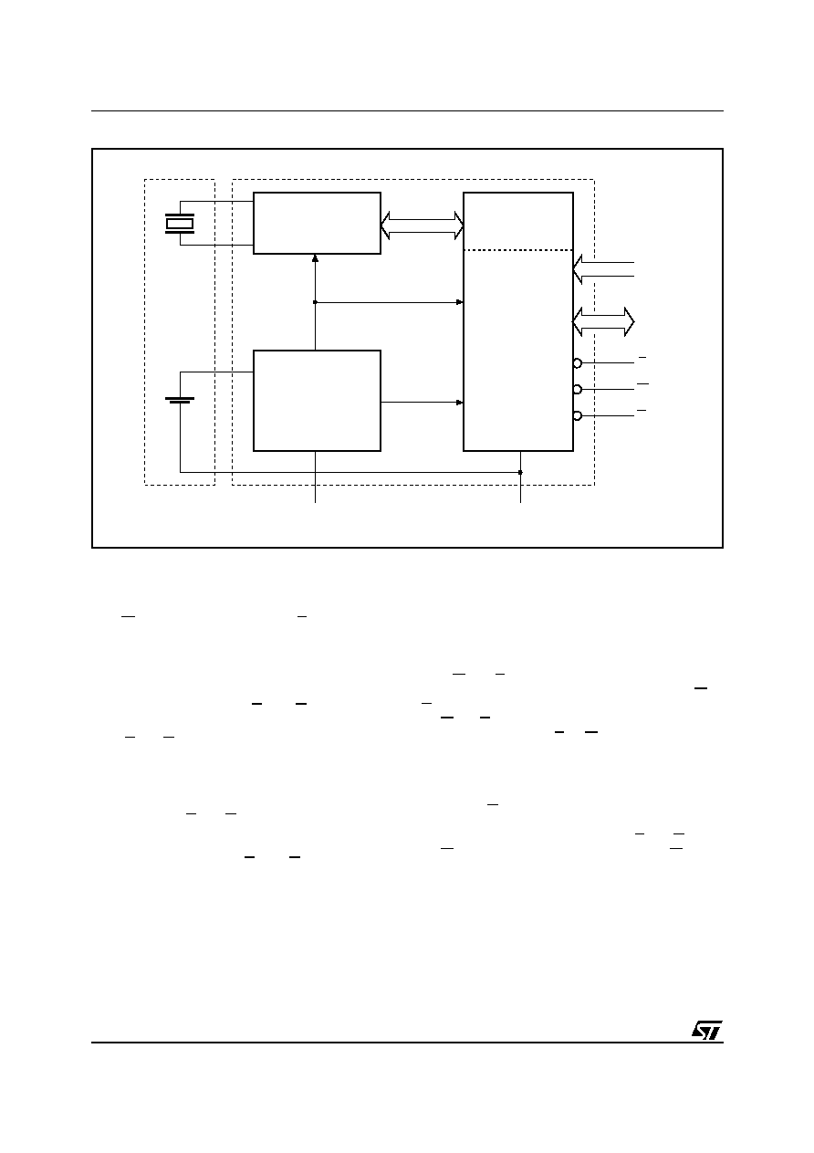
As Figure 3 shows, the static memory array and
the quartz controlled clock oscillator of the
M48T35AY/35AV are integrated on one silicon
chip. The two circuits are interconnected at the up-
per eight memory locations to provide user acces-
sible BYTEWIDETM clock information in the bytes
with addresses 7FF8h-7FFFh.
The clock locations contain the year, month, date,
day, hour, minute, and second in 24 hour BCD for-
mat. Corrections for 28, 29 (leap year), 30, and 31
day months are made automatically. Byte 7FF8h
is the clock control register. This byte controls user
access to the clock information and also stores the
clock calibration setting.
Table 1. Signal Names
A0-A14
Address Inputs
DQ0-DQ7
Data Inputs / Outputs
E
Chip Enable
G
Output Enable
W
Write Enable
V
CC
Supply Voltage
V
SS
Ground
The 28 pin 600mil DIP CAPHATTM houses the
M48T35AY/35AV silicon with a quartz crystal and
a long life lithium button cell in a single package.
The 28 pin 330mil SOIC provides sockets with
gold plated contacts at both ends for direct con-
nection to a separate SNAPHAT housing contain-
ing the battery and crystal. The unique design
allows the SNAPHAT battery package to be
mounted on top of the SOIC package after the
3/19
M48T35AY, M48T35AV
Table 2. Absolute Maximum Ratings
(1)
Note: 1. Stresses greater than those listed under "Absolute Maximum Ratings" may cause permanent damage to the device. This is a stress
rating only and functional operation of the device at these or any other conditions above those indicated in the operational section
of this specification is not implied. Exposure to the absolute maximum rating conditions for extended periods of time may affect
reliability.
2. Soldering temperature not to exceed 260∞C for 10 seconds (total thermal budget not to exceed 150∞C for longer than 30 seconds).
CAUTION: Negative undershoots below ≠0.3V are not allowed on any pin while in the Battery Back-up mode.
Symbol
Parameter
Value
Unit
T
A
Ambient Operating Temperature
Grade 1
0 to 70
∞C
Grade 6
≠40 to 85
∞C
T
STG
Storage Temperature (V
CC
Off, Oscillator Off)
≠40 to 85
∞C
T
SLD
(2)
Lead Solder Temperature for 10 seconds
260
∞C
V
IO
Input or Output Voltages
M48T35AY
≠0.3 to 7
V
M48T35AV
≠0.3 to 4.6
V
V
CC
Supply Voltage
M48T35AY
≠0.3 to 7
V
M48T35AV
≠0.3 to 4.6
V
I
O
Output Current
20
mA
P
D
Power Dissipation
1
W
Table 3. Operating Modes
(1)
Note: 1. X = V
IH
or V
IL
; V
SO
= Battery Back-up Switchover Voltage.
2. See Table 7 for details.
Mode
V
CC
E
G
W
DQ0-DQ7
Power
Deselect
4.5V to 5.5V
or
3.0V to 3.6V
V
IH
X
X
High Z
Standby
Write
V
IL
X
V
IL
D
IN
Active
Read
V
IL
V
IL
V
IH
D
OUT
Active
Read
V
IL
V
IH
V
IH
High Z
Active
Deselect
V
SO
to V
PFD
(min)
(2)
X
X
X
High Z
CMOS Standby
Deselect
V
SO
X
X
X
High Z
Battery Back-up Mode
The eight clock bytes are not the actual clock
counters themselves; they are memory locations
consisting of BiPORTTM read/write memory cells.
The M48T35AY/35AV includes a clock control cir-
cuit which updates the clock bytes with current in-
formation once per second. The information can
be accessed by the user in the same manner as
any other location in the static memory array.
The M48T35AY/35AV also has its own Power-fail
Detect circuit. The control circuitry constantly mon-
itors the single 5V supply for an out of tolerance
condition. When V
CC
is out of tolerance, the circuit
write protects the SRAM, providing a high degree
of data security in the midst of unpredictable sys-
tem operation brought on by low V
CC
. As V
CC
falls
below approximately 3V, the control circuitry con-
nects the battery which maintains data and clock
operation until valid power returns.
M48T35AY, M48T35AV
4/19
READ MODE
The M48T35AY/35AV is in the Read Mode when-
ever W (Write Enable) is high and E (Chip Enable)
is low. The unique address specified by the 15 Ad-
dress Inputs defines which one of the 32,768 bytes
of data is to be accessed. Valid data will be avail-
able at the Data I/O pins within Address Access
time (t
AVQV
) after the last address input signal is
stable, providing that the E and G access times
are also satisfied.
If the E and G access times are not met, valid data
will be available after the latter of the Chip Enable
Access time (t
ELQV
) or Output Enable Access time
(t
GLQV
).
The state of the eight three-state Data I/O signals
is controlled by E and G. If the outputs are activat-
ed before t
AVQV
, the data lines will be driven to an
indeterminate state until t
AVQV
. If the Address In-
puts are changed while E and G remain active,
output data will remain valid for Output Data Hold
time (t
AXQX
) but will go indeterminate until the next
Address Access.
WRITE MODE
The M48T35AY/35AV is in the Write Mode when-
ever W and E are low. The start of a write is refer-
enced from the latter occurring falling edge of W or
E. A write is terminated by the earlier rising edge
of W or E. The addresses must be held valid
throughout the cycle. E or W must return high for
a minimum of t
EHAX
from Chip Enable or t
WHAX
from Write Enable prior to the initiation of another
read or write cycle. Data-in must be valid t
DVWH
prior to the end of write and remain valid for t
WHDX
afterward. G should be kept high during write cy-
cles to avoid bus contention; although, if the output
bus has been activated by a low on E and G, a low
on W will disable the outputs t
WLQZ
after W falls.
Figure 3. Block Diagram
AI01623
LITHIUM
CELL
OSCILLATOR AND
CLOCK CHAIN
VPFD
VCC
VSS
32,768 Hz
CRYSTAL
VOLTAGE SENSE
AND
SWITCHING
CIRCUITRY
8 x 8 BiPORT
SRAM ARRAY
32,760 x 8
SRAM ARRAY
A0-A14
DQ0-DQ7
E
W
G
POWER
5/19
M48T35AY, M48T35AV
DATA RETENTION MODE
With valid V
CC
applied, the M48T35AY/35AV op-
erates as a conventional BYTEWIDE static RAM.
Should the supply voltage decay, the RAM will au-
tomatically power-fail deselect, write protecting it-
self when V
CC
falls within the V
PFD
(max), VPFD
(min) window. All outputs become high imped-
ance, and all inputs are treated as "don't care."
Note: A power failure during a write cycle may cor-
rupt data at the currently addressed location, but
does not jeopardize the rest of the RAM's content.
At voltages below V
PFD
(min), the user can be as-
sured the memory will be in a write protected state,
provided the V
CC
fall time is not less than t
F
. The
M48T35AY/35AV may respond to transient noise
spikes on V
CC
that reach into the deselect window
during the time the device is sampling V
CC
. There-
fore, decoupling of the power supply lines is rec-
ommended.
When V
CC
drops below V
SO
, the control circuit
switches power to the internal battery which pre-
serves data and powers the clock. The internal
button cell will maintain data in the M48T35AY/
35AV for an accumulated period of at least 7 years
when V
CC
is less than V
SO
. As system power re-
turns and V
CC
rises above V
SO
, the battery is dis-
connected, and the power supply is switched to
external V
CC
. Write protection continues until V
CC
reaches V
PFD
(min) plus t
REC
(min). E should be
kept high as V
CC
rises past V
PFD
(min) to prevent
inadvertent write cycles prior to processor stabili-
zation. Normal RAM operation can resume t
REC
after V
CC
exceeds V
PFD
(max).
Also, as V
CC
rises, the battery voltage is checked.
If the voltage is less than approximately 2.5V, an
internal Battery Not OK (BOK) flag will be set. The
BOK flag can be checked after power up. If the
BOK flag is set, the first write attempted will be
blocked. The flag is automatically cleared after the
first write, and normal RAM operation resumes.
Figure 9 illustrates how a BOK check routine could
be structured.
For more information on Battery Storage Life refer
to the Application Note AN1012.
CLOCK OPERATIONS
Reading the Clock
Updates to the TIMEKEEPER registers should be
halted before clock data is read to prevent reading
data in transition. Because the BiPORT TIME-
KEEPER cells in the RAM array are only data reg-
isters, and not the actual clock counters, updating
the registers can be halted without disturbing the
clock itself.
Updating is halted when a '1' is written to the
READ bit, D6 in the Control Register 7FF8h. As
long as a '1' remains in that position, updating is
halted.
After a halt is issued, the registers reflect the
count; that is, the day, date, and the time that were
current at the moment the halt command was is-
sued.
All of the TIMEKEEPER registers are updated si-
multaneously. A halt will not interrupt an update in
progress. Updating is within a second after the bit
is reset to a '0'.
Table 4. AC Measurement Conditions
Note that Output Hi-Z is defined as the point where data is no longer
driven.
Input Rise and Fall Times
5ns
Input Pulse Voltages
0 to 3V
Input and Output Timing Ref. Voltages
1.5V
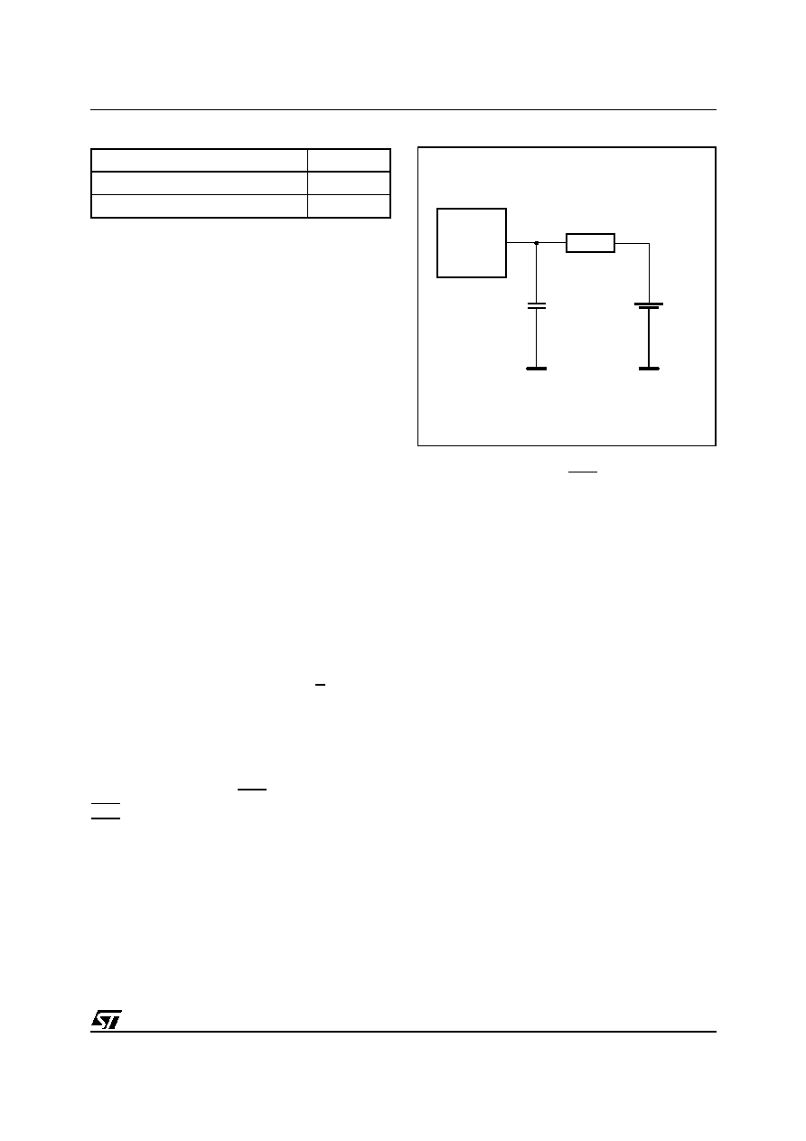
Figure 4. AC Testing Load Circuit
AI02586
CL = 100pF
(or 5pF)
CL includes JIG capacitance
645
DEVICE
UNDER
TEST
1.75V