M54HC03
M74HC03
January 1993
QUAD 2-INPUT OPEN DRAIN NAND GATE
B1R
(Plastic Package)
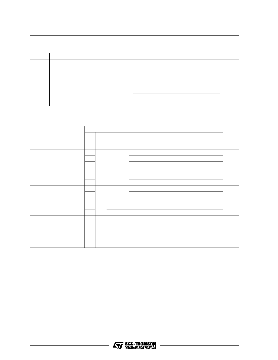
ORDER CODES :
M54HC03F1R
M74HC03M1R
M74HC03B1R
M74HC03C1R
F1R
(Ceramic Package)
M1R
(Micro Package)
C1R
(Chip Carrier)
PIN CONNECTIONS (top view)
NC =
No Internal
Connection
INPUT AND OUTPUT EQUIVALENT CIRCUIT
.
HIGH SPEED
t
PZ
= 5 ns (TYP.) AT V
CC
= 5 V
.
LOW POWER DISSIPATION
I
CC
= 1
�
A (MAX.) AT T
A
= 25
�
C
.
HIGH NOISE IMMUNITY
V
NIH
= V
NIL
= 28 % V
CC
(MIN.)
.
OUTPUT DRIVE CAPABILITY
10 LSTTL LOADS
.
BALANCED PROPAGATION DELAYS
t
PLH
= t
PHL
.
WIDE OPERATING VOLTAGE RANGE
V
CC
(OPR) = 2 V TO 6 V
.
PIN AND FUNCTION COMPATIBLE WITH
54/74LS03
The M54/74HC03 is a high speed CMOS QUAD 2-
INPUT OPEN DRAIN NAND GATE fabricated in sili-
con gate C
2
MOS technology.
It has the same high speed performance of LSTTL
combined with true CMOS low power consumption.
The internal circuit is composed of 3 stages includ-
ing buffer output, which gives high noise immunity
and stable output. This device can, with an external
pull-up resistor, be used in wired AND configuration.
This device can be also used as a led driver and in
any other application requiring a current sink. All in-
puts are equipped with protection circuits against
static discharge and transient excess voltage.
DESCRIPTION
1/9
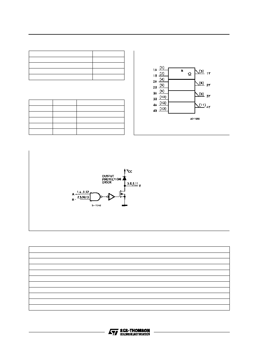
TRUTH TABLE
A
B
Y
L
L
Z
L
H
Z
H
L
Z
H
H
L
Z = HIGH IMPEDANCE
PIN DESCRIPTION
PIN No
SYMBOL
NAME AND FUNCTION
1, 4, 9, 12
1A to 4A
Data Inputs
2, 5, 10, 13
1B to 4B
Data Inputs
3, 6, 8, 11
1Y to 4Y
Data Outputs
7
GND
Ground (0V)
14
V
CC
Positive Supply Voltage
IEC LOGIC SYMBOL
CIRCUIT DIAGRAM
VCC = Pin 14
GND = Pin 7
open�drain outputs
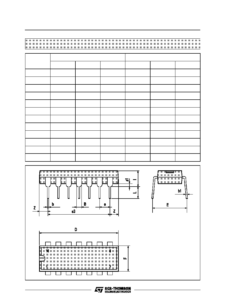
ABSOLUTE MAXIMUM RATINGS
Symbol
Parameter
Value
Unit
V
CC
Supply Voltage
-0.5 to +7
V
V
I
DC Input Voltage
-0.5 to V
CC
+ 0.5
V
V
O
DC Output Voltage
-0.5 to V
CC
+ 0.5
V
I
IK
DC Input Diode Current
�
20
mA
I
OK
DC Output Diode Current
�
20
mA
I
O
DC Output Sink Current Per Output Pin
+ 25
mA
I
CC
or I
GND
DC V
CC
or Ground Current
�
50
mA
P
D
Power Dissipation
500 (*)
mW
T
stg
Storage Temperature
-65 to +150
o
C
T
L
Lead Temperature (10 sec)
300
o
C
Absolute Maximum Ratings are those values beyond which damage to the device may occur. Functional operation under these condition is not implied.
(*) 500 mW:
65
o
C derate to 300 mW by 10mW/
o
C: 65
o
C to 85
o
C
M54/M74HC03
2/9
AC ELECTRICAL CHARACTERISTICS (C
L
= 50 pF, Input t
r
= t
f
= 6 ns)
Symbol
Parameter
Test Conditions
Value
Unit
V
CC
(V)
T
A
= 25
o
C
54HC and 74HC
-40 to 85
o
C
74HC
-55 to 125
o
C
54HC
Min.
Typ.
Max.
Min.
Max.
Min.
Max.
t
TLH
t
THL
Output Transition
Time
2.0
30
75
95
110
ns
4.5
8
15
19
22
6.0
7
13
16
19
t
PLZ
Propagation
Delay Time
2.0
RL = 1 K
16
60
75
90
ns
4.5
9
12
15
18
6.0
8
10
13
15
t
PZL
Propagation
Delay Time
2.0
R
L
= 1 K
23
60
75
90
ns
4.5
7
12
15
18
6.0
6
10
13
15
C
IN
Input Capacitance
5
10
10
10
pF
C
PD
(*)
Power Dissipation
Capacitance
7
pF
(*) C
PD
is defined as the value of the IC's internal equivalent capacitance which is calculated from the operating current consumption without load.
(Refer to Test Circuit). Average operting current can be obtained by the following equation. I
CC
(opr) = C
PD
�
V
CC
�
f
IN
+ I
CC
/4 (per Gate)
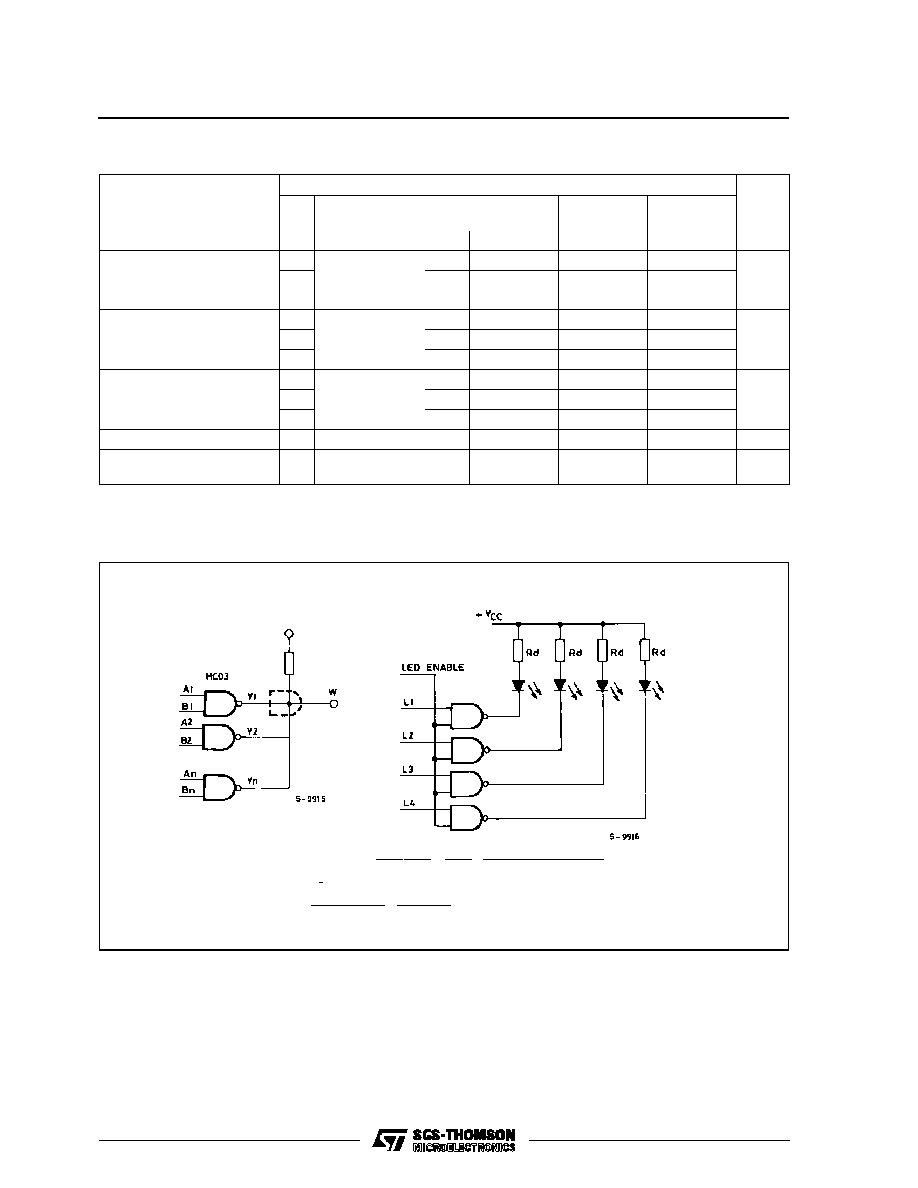
W = Y1 Y2 ... Yn = A1B1 A2B2 ... AnBn = A1B1 + A2B2 +... + AnBn
I
D
= 10 : 20 mA
R
D
=
V
CC
-
V
D
-
V
DS
I
D
=
5
-
2
-
0.4
20
�
10
-
3
=
130
(*)
(*) 260
with I
D
= 10 mA
TYPICAL APPLICATIONS
Wired AND
LED Driver with Blanking
Typical values
V
CC
= 5V
V
D
= 2V
V
DS
= 0.4V
R
D
= 120
�
270
M54/M74HC03
4/9