L9704
March 1992
OCTAL SUPPLY CONTACT MONITORING CIRCUIT
.
OPERATING DC SUPPLY VOLTAGE RANGE
5V TO 25V
.
SUPPLY OVERVOLTAGE PULSE UP TO 40V
.
VERY LOW STANDBY QUIESCENT CUR-
RENT 0.2mA
.
INTERNAL CLAMPING DIODES AT CONTACT
INPUTS TO V
S
AND GND
.
INPUT PULSE CURRENT CAPABILITY UP TO
+ 50mA, ≠ 75mA
.
NOMINAL CONTACT CURRENTS OF 10mA
DEFINED BY EXTERNAL CONTACT SERIES
RESISTORS R
IN1-8
.
CONTACT STATUS MONITORING BY COM-
PARING THE RESISTANCE AT CONTACT
SENSEINPUTS WITH THE INTERNAL REFER-
ENCE RESISTOR VALUE
.
HIGH IMMUNITY DUE TO RESISTANCE COM-
PARISON WITH HYSTERESIS
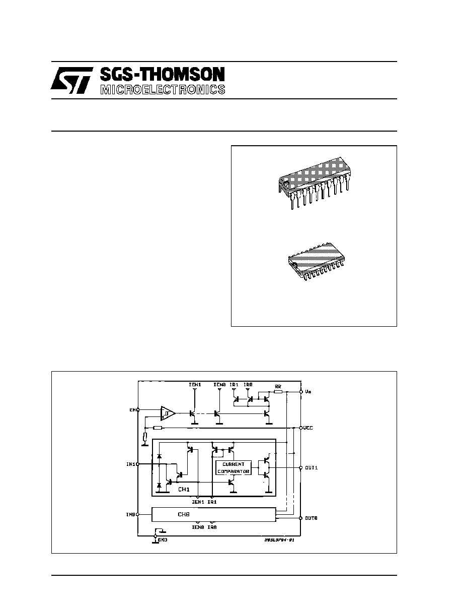
ORDERING NUMBERS: L9704 (DIP≠20)
L9704D (SO≠20L)
DIP≠20
SO≠20L
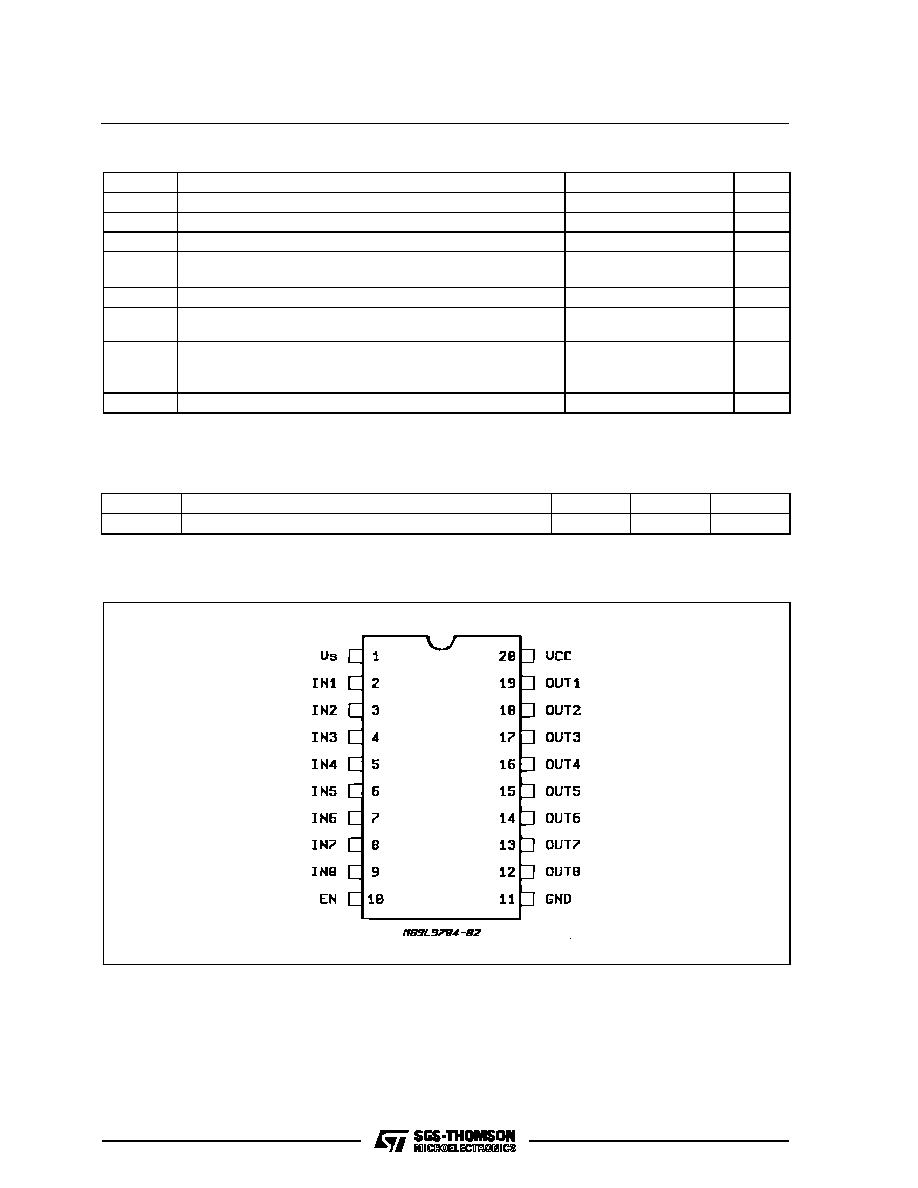
DESCRIPTION
The L9704 is a bipolar monolithic integrated circuit
for monitoring the status of up to eight contactscon-
nected to the power supply (battery).
It contains eight contact sense inputs and eight mi-
crocomputer compatible three-state outputs.
BLOCK DIAGRAM
1/8
ABSOLUTE MAXIMUM RATINGS
Symbol
Parameter
Test Conditions
Unit
V
S
Transient Supply Voltage (t
1s)
+40
V
V
CC
Logic Supply Voltage
7
V
I
IN DC
Input DC Current
±
40
mA
I
INP
Input DC Pulse
(test pulse specification: 0 < tP < 2ms, f
0.2Hz, n = 25000)
50
-75
mA
mA
I
O
Output Current
Internally Limited
V
EN
Enable Input Voltage
V
CC
+0.3
-0.3
V
V
P
O
Power Dissipation at T
amb
= 80
∞
C
DIP20
SO20
875
420
mW
mW
T
stg,
T
J
Storage and Junction Temperature Range
-55 to 150
∞
C
PIN CONNECTION (top view)
THERMAL DATA
Symbol
Parameter
DIP20
SO20
Unit
R
th j-amb
Thermal Resistance Junction to Ambient
MAX.
80
165
∞
C/W
L9704
2/8
ELECTRICAL CHARACTERISTICS (5V
V
S
25V; -40
∞
C
T
j
125
∞
C; 4.75V
V
CC
5.25V unless
otherwise specified; the currents flowing in the arrow direction are assumed positive as marked in the
application circuit diagram, fig. 1).
Symbol
Parameter
Test Conditions
Min.
Typ.
Max.
Unit
V
ENL
Enable Input Voltage LOW
(device activated)
0.8
V
V
ENH
Enable Input Voltage HIGH
2.4
V
V
EN hyst
Enable Input Hysteresis
200
300
800
mV
I
EN
Enable Input Current
2.4V < V
EN
< V
CC
5
µ
A
0V < V
EN
< 0.8V
-5
-1
µ
A
V
OUTH
Output Voltage HIGH
0 < I
OUT
< 100
µ
A
4.0
V
CC
-0.1
V
CC
V
V
OUTL
Output Voltage LOW
I
OUT
= -1mA
0.05
0.2
0.4
V
I
OUT TS
Output TRISTATE Current
0 < V
OUT
< V
CC
0.5
µ
A
V
IN
Input Voltage (device active)
EN = LOW
R
IN
= 1k
0.4
1.5
2
V
V
IN
Input Voltage During Clamping
(device disabled)
EN = HIGH
I
IN
= 30mA
I
IN
= -30mA
V
S
+ 0.3
-2
V
S
+ 1
-1
V
S
+ 2
-0.3
V
V
I
OUT
Output Current
OUT = HIGH
V
OUT
= 0
2
mA
I
OUT
Output Current
OUT = LOW
VOUT = 5.5V
-20
mA
R
IL
Input Resistor (note 1)
LOW Threshold
5V < V
S
< 16V
V
GND
0.1V
S
1.1
4.8
K
R
IH
Input Resistor (note 1)
HIGH Threshold
6.5
29
K
Input Resistor
Threshold Ratio (note1)
0.65
0.75
0.85
I
QC
Quiescent Current
EN = HIGH (t
ENH
80
µ
s)
5V < V
S
< 16V
-40
∞
C
T
j
100
∞
C
All Inputs Open
0.12
0.16
mA
I
QS
0.04
mA
SI
IN
2)
Input Leakage Current
All Inputs Closed V
BAT
V
D1
0.24
mA
I
QC
I
QS
Quiescent Current
EN = LOW
13
2
mA
mA
t
do
Delay Time/Output
(EN LOW to output data ready)
C
OUT
50pF
15
+3R
IN
C
IN
µ
s
t
dTS
Delay Time/Tristate
(EN HIGH to output TRISTAT E)
C
OUT
50pF
10
µ
s
Notes :
1. The input resi stor threshold valu e is a resistor value from the IN≠pin to battery at which the corresponding output changes
its status (see fig. 3)
2: SI
IN
is the sum of the in put curr ents SI
IN
=
i
=
1
8
I
IN1
.
R
IL
R
IH
L9704
3/8

APPLICATION CIRCUIT DIAGRAM
Figure 1 : Typical application diagram for the L9704 circuit. The current flowing in the arrow direction is as-
sumed positive. The external capacitors C
IN
and C
OUT
represent the total wiring capacitance at
the corresponding pins.
FUNCTIONAL DESCRIPTION
The L9704 circuit monitors the status of the contacts
connectedto battery and through the series external
resistors R
IN
to the contact sense input pins. The
contacts equivalent circuit is supposed to be as
shown in fig. 2.
The L9704 circuit compares the input current with
the current through the internal reference resistor.
The device is designed to work with an externalinput
series resistor of R
IN1-8
= 1k
. With this input resistor
the contact current, when the contact is closed and
the device activated (EN = LOW) is
V
BAT
+
V
BAT
≠ 2V
I
IN
=
1K
(1)
For this calculation the limit value of the V
IN
(satura-
tion voltage of 2V) was considered so that the lowest
limit value of I
IN
is calculated in (1).
The function of the circuit can be demonstrated with
the transfer characteristics, showing the output
status as a function of the input resistor R
I
, shown
in figure 3. The input resistor is a sum of the R
IN
and
the contactresistance R
CON
or R
COFF
, for the closed
contact :
R
I
= R
IN
+ R
CON
,
(2)
and for the open contact :
R
I
= R
IN
+ R
COFF
.
(3)
The output goes HIGH when the input resistance in-
creases above 6.5k
(typical value) and goesLOW,
when the input resistance decreases below 4.8K
(typical value). The limit values of R
I
= 1.1K
for
LOW and R
I
= 29k
for HIGH implies that a contact
with R
CON
= 100
(at I
IN
= 10mA) will be recognized
as ON = LOW and a contact with R
COFF
= 28k
will
be recognized as OFF = HIGH. These limits are
valid within the supply voltage range 5V
V
s
16V,
the
battery
voltage
potential
difference
of
VBAT
0.1V
BAT
and the variation of the reverse
battery protection diode D1 voltage from 0.5V to 1V.
L9704
4/8

The internal clamping diodes at the contact monitor-
ing inputs, together with the external contact series
resistors R
IN
, allows the device to withstand tran-
sients at the contact connection. The contact series
resistor R
IN
limits the input current at the transient.
The dynamic behaviour of the circuit is defined by
the times t
do
and t
dTS
. When the contact becomes
open, the input capacitor C
IN
must be charged
through the resistor R
IN
. In this case the total delay
time may also be influenced by the time constant R
IN
C
IN
. The delay time t
dTS
, when disabling the device
is defined only by the internal circuitry. In bothcases,
an externaloutput capacitanceless than 50pF is as-
sumed, the internal output capacitances of the
three-state buffers are less than 5pF.
Figure 2 : The Contact Sense Input Connection with the Contact Equivalent Circuit.
Figure 3 : The Output Voltage as a Function of the Input Resistance at the Corresponding Contact Sense
Input.
L9704
5/8