M54HC123/123A
M74HC123/123A
October 1993
DUAL RETRIGGERABLE MONOSTABLE MULTIVIBRATOR
B1R
(Plastic Package)
ORDER CODES :
M54HCXXXF1R
M74HCXXXM1R
M74HCXXXB1R
M74HCXXXC1R
F1R
(Ceramic Package)
M1R
(Micro Package)
C1R
(Chip Carrier)
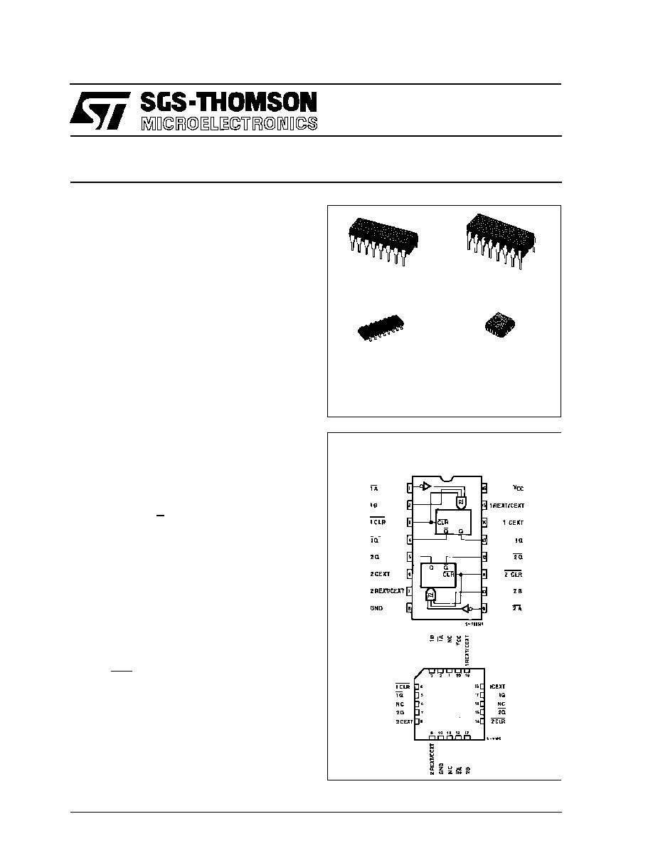
PIN CONNECTIONS (top view)
NC =
No Internal
Connection
.
HIGH SPEED
t
PD
= 25 ns (TYP) at V
CC
= 5V
.
LOW POWER DISSIPATION
STANDBY STATE I
CC
=4
µ
A (MAX.) AT T
A
=25
∞
C
ACTIVE STATE I
CC
= 200
µ
A (TYP.) AT V
CC
=5V
.
HIGH NOISE IMMUNITY
V
NIH
= V
NIL
= 28 % V
CC
(MIN.)
.
OUTPUT DRIVE CAPABILITY
10 LSTTL LOADS
.
SYMMETRICAL OUTPUT IMPEDANCE
I
OH
= I
OL
= 4 mA (MIN.)
.
BALANCED PROPAGATION DELAYS
t
PLH
= t
PHL
.
WIDE OPERATING VOLTAGE RANGE
V
CC
(OPR) = 2 V TO 6 V
.
WIDE OUTPUT PULSE WIDTH RANGE
t
WOUT
= 120 ns
60 s OVER AT V
CC
= 4.5 V
.
PIN AND FUNCTION COMPATIBLE WITH
54/74LS123
The M54/74HC123 is a high speed CMOS MONO-
STABLE multivibrator fabricated with silicon gate
C
2
MOS technology. It achieves the high speed
operation similar to equivalent LSTTL while main-
taining the CMOS low power dissipation. There are
two trigger inputs, A INPUT (negative edge) and 8
INPUT (positive edge). These inputs are valid for
slow rising/falling signals, (tr = tf = I sec). The device
may also be triggered by using the CLR input (posi-
tive-edge) because of the Schmitt-trigger input ;
after triggering the output maintains the MONO-
STABLE state for the time period determined by the
external resistor Rx and capacitor Cx. When Cx
10nF and Rx
10K
, the output pulse width value
is approssimatively given by the formula: t
w(out)
= K
∑
Cx
∑
Rx.
Two different pulse width constant are available:
K
0.45 for HC123
K
1 for HC123A.
Taking CLR low breaks this MONOSTABLE
STATE. If the next trigger pulse occurs during the
MONOSTABLEperiod it makes the MONOSTABLE
period longer. Limit for values of Cx and Rx :
Cx : NO LIMIT
Rx : V
CC
< 3.0 V 5 K
to 1 M
V
CC
3.0 V 1 K
to 1 M
All inputs are equipped with protection circuits
DESCRIPTION
1/14
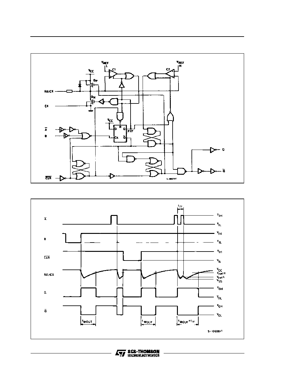
SYSTEM DIAGRAM
TIMING CHART
M54/M74HC123/123A
2/14
BLOCK DIAGRAM
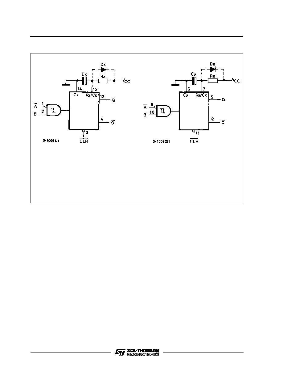
Note :
(1) Cx, Rx, Dx are external components.
(2) Dx is a clamping diode.
The external capacitor is charged to V
CC
inthe stand-by state, i.e. no trigger. When the supply voltage is turned off Cx is discharged mainly
through an internal parasitic diode (see figures). If Cx is sufficiently large and V
CC
decreases rapidy, there will be some possibility of da-
maging the I.C. with a surge current or latch-up. If the voltage supply filter capacitor is large enough and V
CC
decrease slowly, the surge
current is automatically limited and damage the I.C. is avoided. The maximum forward current of the parasitic diode is approximately 20
mA. In cases where Cx is large the time taken for the supply voltage to fall to 0.4 V
CC
can be calculated as follows :
t
f
(V
CC
≠ 0.7)
Cx/20mA
In cases where t
f
is too short an external clamping diode is required to protect the I.C. from the surge current.
FUNCTIONAL DESCRIPTION
STAND-BY STATE
The external capacitor, Cx, is fully charged to V
CC
in the stand-by state. Hence, before triggering, tran-
sistor Qp and Qn (connected to the Rx/Cx node) are
both turned-off. The two comparators that control
the timing and the two reference voltage sources
stop operating. The total supply current is therefore
only leakage current.
TRIGGER OPERATION
Triggering occurs when :
1 st) A is "low" and B has a falling edge ;
2 nd) B is "high" and A has a rising edge ;
3 rd) A is low and B is high and C1 has a rising edge.
After the multivibrator has been retriggered com-
parator C1 and C2 start operating and Qn is turned
on. Cx then discharges through Qn. The voltage at
the node R/C external falls.
When it reaches V
REFL
the output of comparator C1
becomes low. This in turn resets the flip-flop and Qn
is turned off.
At this point C1 stops functioning but C2 continues
to operate.
The voltage at R/C external begins to rise with a time
constant set by the external components Rx, Cx.
Triggering the multivibrator causes Q to go high after
internal delay due to the flip-flop and the gate. Q re-
mains high until the voltage at R/C external rises
again to V
REFH
. At this point C2 output goes low and
O goes low. C2 stop operating. That means that
after triggering when the voltage R/C external re-
turns to V
REFH
the multivibrator has returned to its
MONOSTABLE STATE. In the case where Rx
Cx
are large enough and the discharge time of the ca-
pacitor and the delay time in the I.C. can be ignored,
the width of the output pulse tw (out) is as follows :
t
W(OUT)
= 0.46 Cx
Rx (HC123)
t
W(OUT)
= Cx
Rx (HC123A)
M54/M74HC123/123A
3/14
FUNCTIONAL DESCRIPTION (continued)
RE-TRIGGERED OPERATION
When a second trigger pulse follows the first its ef-
fect will depend on the state of the multivibrator. If
the capacitor Cx is being charged the voltage level
of R/C external falls to Vrefl again and Q remains
high i.e. the retrigger pulse arrives in a time shorter
than the period Rx
Cx seconds, the capacitor
charging time constant. If the second trigger pulse
is very close to the initial trigger pulse it is ineffective
; i.e. the second trigger must arrive in the capacitor
discharge cycle to be ineffective; Hence the mini-
mum time for a second trigger to be effective de-
pends on V
CC
and Cx.
RESET OPERATION
CL is normally high. If CL is low, the trigger is not ef-
fective because Q output goes low and trigger con-
trol flip-flop is reset.
Also transistor Op is turned on and Cx is charged
quicky to V
CC
. This means if CL input goes low, the
IC becomes waiting state both in operating and non
operating state.
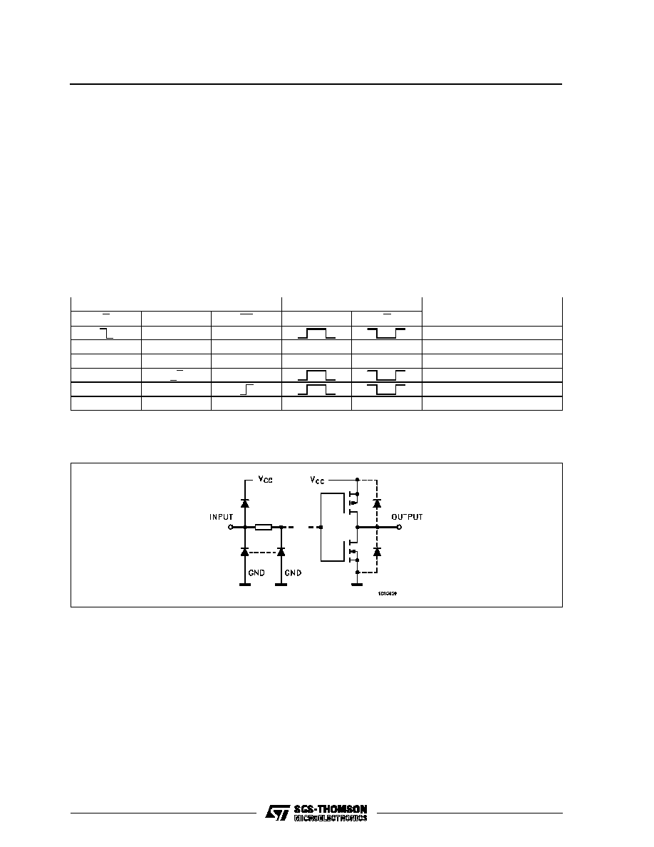
TRUTH TABLE
INPUTS
OUTPUTS
NOTE
A
B
CL
Q
Q
H
H
OUTPUT ENABLE
X
L
H
L
H
INHIBIT
H
X
H
L
H
INHIBIT
L
H
OUTPUT ENABLE
L
H
OUTPUT ENABLE
X
X
L
L
H
INHIBIT
X: Don't Care Z: High Impedance
INPUT AND OUTPUT EQUIVALENT CIRCUIT
M54/M74HC123/123A
4/14
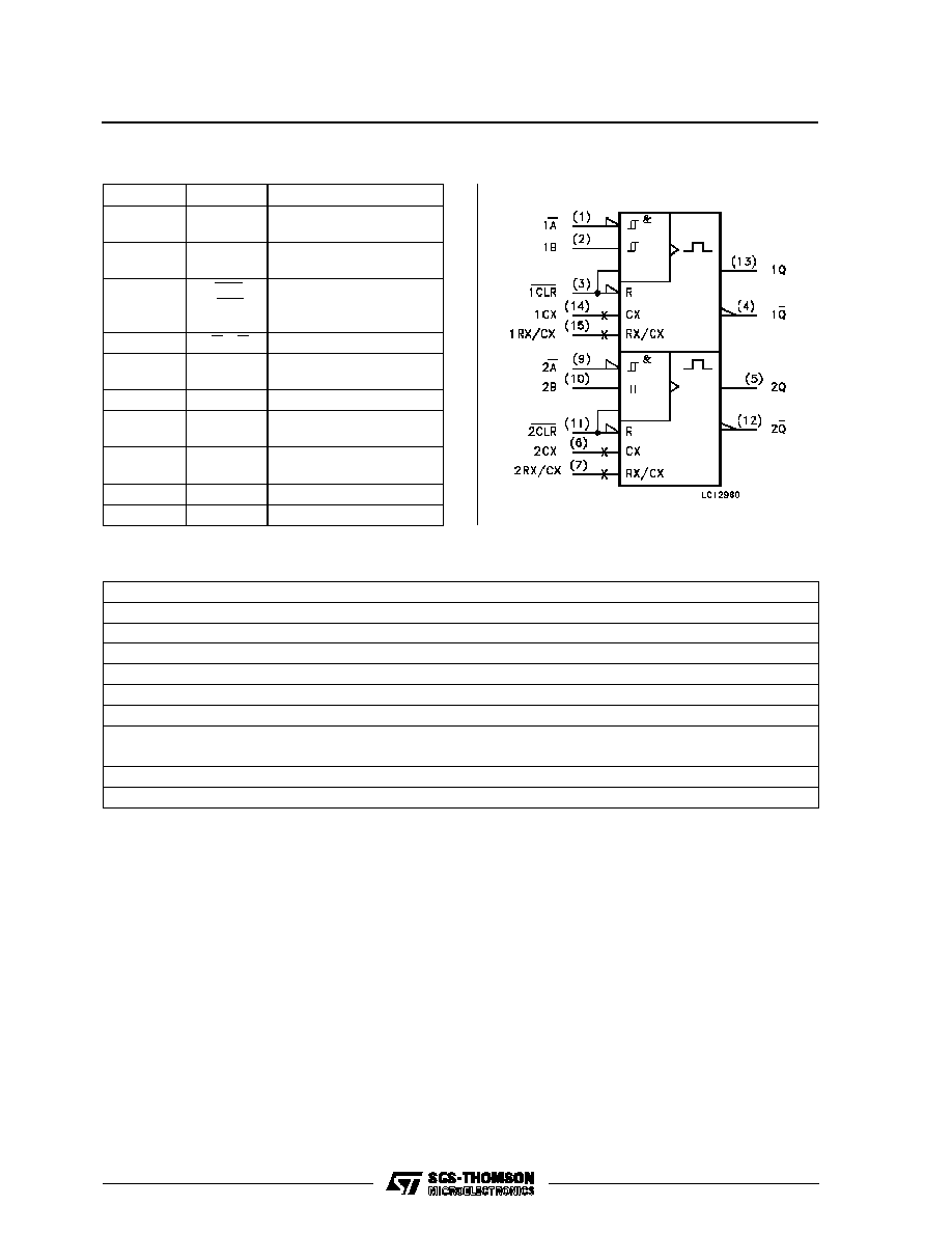
PIN DESCRIPTION
PIN No
SYMBOL
NAME AND FUNCTION
1, 9
1A, 2A
Trigger Inputs (Negative
Edge Triggered)
2, 10
1B, 2B
Trigger Inputs (Positive
Edge Triggered)
3, 11
1CLR,
2CLR
Direct Reset LOW and
Trigger Action at Positive
Edge
4, 12
1Q, 2Q
Outputs (Active LOW)
7
2R
EXT
/C
EXT
External Resistor
Capacitor Connection
13, 5
1Q, 2Q
Outputs (Active HIGH)
14, 6
1C
EXT
2C
EXT
External Capacitor
Connection
15
1R
EXT
/C
EXT
External Resistor
Capacitor Connection
8
GND
Ground (0V)
16
V
CC
Positive Supply Voltage
IEC LOGIC SYMBOL
ABSOLUTE MAXIMUM RATING
Symbol
Parameter
Value
Unit
V
CC
Supply Voltage
-0.5 to +7
V
V
I
DC Input Voltage
-0.5 to V
CC
+ 0.5
V
V
O
DC Output Voltage
-0.5 to V
CC
+ 0.5
V
I
IK
DC Input Diode Current
±
20
mA
I
OK
DC Output Diode Current
±
20
mA
I
O
DC Output Source Sink Current Per Output Pin
±
25
mA
I
CC
or I
GND
DC V
CC
or Ground Current
±
50
mA
P
D
Power Dissipation
500 (*)
mW
T
stg
Storage Temperature
-65 to +150
o
C
T
L
Lead Temperature (10 sec)
300
o
C
Absolute Maximum Ratings are those values beyond which damage to the device may occur. Functional operation under these condition is not implied.
(*) 500 mW:
65
o
C derate to 300 mW by 10mW/
o
C: 65
o
C to 85
o
C
M54/M74HC123/123A
5/14
DC SPECIFICATIONS
Symbol
Parameter
Test Conditions
Value
Unit
V
CC
(V)
T
A
= 25
o
C
54HC and 74HC
-40 to 85
o
C
74HC
-55 to 125
o
C
54HC
Min.
Typ.
Max.
Min.
Max.
Min.
Max.
V
IH
High Level Input
Voltage
2.0
1.5
1.5
1.5
V
4.5
3.15
3.15
3.15
6.0
4.2
4.2
4.2
V
IL
Low Level Input
Voltage
2.0
0.5
0.5
0.5
V
4.5
1.35
1.35
1.35
6.0
1.8
1.8
1.8
V
OH
High Level
Output Voltage
2.0
V
I
=
V
IH
or
V
IL
I
O
=-20
µ
A
1.9
2.0
1.9
1.9
V
4.5
4.4
4.5
4.4
4.4
6.0
5.9
6.0
5.9
5.9
4.5
I
O
=-4.0 mA
4.18
4.31
4.13
4.10
6.0
I
O
=-5.2 mA
5.68
5.8
5.63
5.60
V
OL
Low Level Output
Voltage
2.0
V
I
=
V
IH
or
V
IL
I
O
= 20
µ
A
0.0
0.1
0.1
0.1
V
4.5
0.0
0.1
0.1
0.1
6.0
0.0
0.1
0.1
0.1
4.5
I
O
= 4.0 mA
0.17
0.26
0.33
0.40
6.0
I
O
= 5.2 mA
0.18
0.26
0.33
0.40
I
I
Input Leakage
Current
6.0
V
I
= V
CC
or GND
±
0.1
±
1
±
1
µ
A
I
I
R/C Terminal Off
State Current
6.0
V
I
= V
CC
or GND
±
0.1
±
1
±
1
µ
A
I
CC
Quiescent Supply
Current
6.0
V
I
= V
CC
or GND
4
40
80
µ
A
I
CC
'
Active State
Supply Current (1)
2.0
V
I
= V
CC
or GND
Pin 7 or 15
V
IN
= V
CC
/2
45
200
260
320
µ
A
4.5
500
600
780
960
µ
A
6.0
0.7
1
1.3
1.6
mA
(1): Per Circuit
RECOMMENDED OPERATING CONDITIONS
Symbol
Parameter
Value
Unit
V
CC
Supply Voltage
2 to 6
V
V
I
Input Voltage
0 to V
CC
V
V
O
Output Voltage
0 to V
CC
V
T
op
Operating Temperature: M54HC Series
M74HC Series
-55 to +125
-40 to +85
o
C
o
C
t
r
, t
f
Input Rise and Fall Time
0 to 1000
ns
0 to 500
0 to 400
C
X
External Capacitor
NO LIMITATION
pF
R
X
External Resistor
V
CC
< 3 V
5K to 1M
V
CC
3 V
1K to 1M
(*) The maximum allowable values of Cx and Rx are a function of leakage of capacitor Cx, the leakage of device and leakage due to the board
layout and surface resistance. Susceptibility to externally induced noise may occur for Rx > 1M
M54/M74HC123/123A
6/14

AC ELECTRICAL CHARACTERISTICS (C
L
= 50 pF, Input t
r
= t
f
= 6 ns)
Symbol
Parameter
Test Conditions
Value
Unit
V
CC
(V)
T
A
= 25
o
C
54HC and 74HC
-40 to 85
o
C
74HC
-55 to 125
o
C
54HC
Min.
Typ.
Max.
Min.
Max.
Min.
Max.
t
TLH
t
THL
Output Transition
Time
2.0
30
75
95
110
ns
4.5
8
15
19
22
6.0
7
13
16
19
t
PLH
t
PHL
Propagation
Delay Time
(A, B - Q, Q)
2.0
102
210
265
315
ns
4.5
29
42
53
63
6.0
22
36
45
54
t
PLH
t
PHL
Propagation
Delay Time
(CLRTRIGGER- Q,Q)
2.0
102
235
295
355
ns
4.5
31
47
59
71
6.0
23
40
50
60
t
PLH
t
PHL
Propagation
Delay Time
(CLR - Q, Q)
2.0
68
160
200
240
ns
4.5
20
32
40
48
6.0
16
27
34
41
t
WOUT
Output Pulse
Width
(for HC123)
2.0
C
X
= 100 pF
R
X
= 10 K
1.4
µ
s
4.5
1.2
6.0
1.1
2.0
C
X
= 0.1
µ
F
R
X
= 100 K
4.6
ms
4.5
4.4
6.0
4.3
t
WOUT
Output Pulse
Width
(for HC123A)
2.0
C
X
= 100 pF
R
X
= 10 K
1.9
µ
s
4.5
1.6
6.0
1.5
2.0
C
X
= 0.1
µ
F
R
X
= 100 K
9.8
ms
4.5
9.5
6.0
9.4
t
WOUT
Output Pulse
Width Error
Between Circuits
in Same Package
±
1
%
t
W(H)
t
W(L)
Minimum Pulse
Width
2.0
75
95
110
ns
4.5
15
19
22
6.0
13
16
19
t
W(L)
Minimum Pulse
Width (CLR)
2.0
75
95
110
ns
4.5
15
19
22
6.0
13
16
19
t
rr
Minimum
Retrigger Time
2.0
C
X
= 100 pF
R
X
= 1 K
325
ns
4.5
108
6.0
78
2.0
C
X
= 0.1
µ
F
R
X
= 100 K
5
µ
s
4.5
1.4
6.0
1.2
C
IN
Input Capacitance
5
10
10
10
pF
C
PD
(*)
Power Dissipation
Capacitance
162
pF
(*) C
PD
is defined as the value of the IC's internal equivalent capacitance which is calculated from the operating current consumption without load.
(RefertoTestCircuit). Average operting current canbeobtained by the following equation. I
CC
(opr) =C
PD
∑
V
CC
∑
f
IN
+I
CC
' Duty/100 + I
C
/2 (per monostable)
(I
CC
': Active Supply Current) (Duty:%)
M54/M74HC123/123A
7/14

Output Pulse Width Constant Characteristics
(for HC123)
Output Pulse Width Characteristics (for HC123)
Output Pulse Width Constant Characteristics
(for HC123A)
Output Pulse Width Characteristics (for HC123A)
M54/M74HC123/123A
8/14

TEST CIRCUIT I
CC
(Opr)
* TRANSITION TIME OF INPUT WAVEFORM IS THE SAME AS
THAT IN SASE OF SWITCHINGCHARACTERISTICS TESTS.
SWITCHING CHARACTERISTICS TEST WAVEFORM
M54/M74HC123/123A
9/14
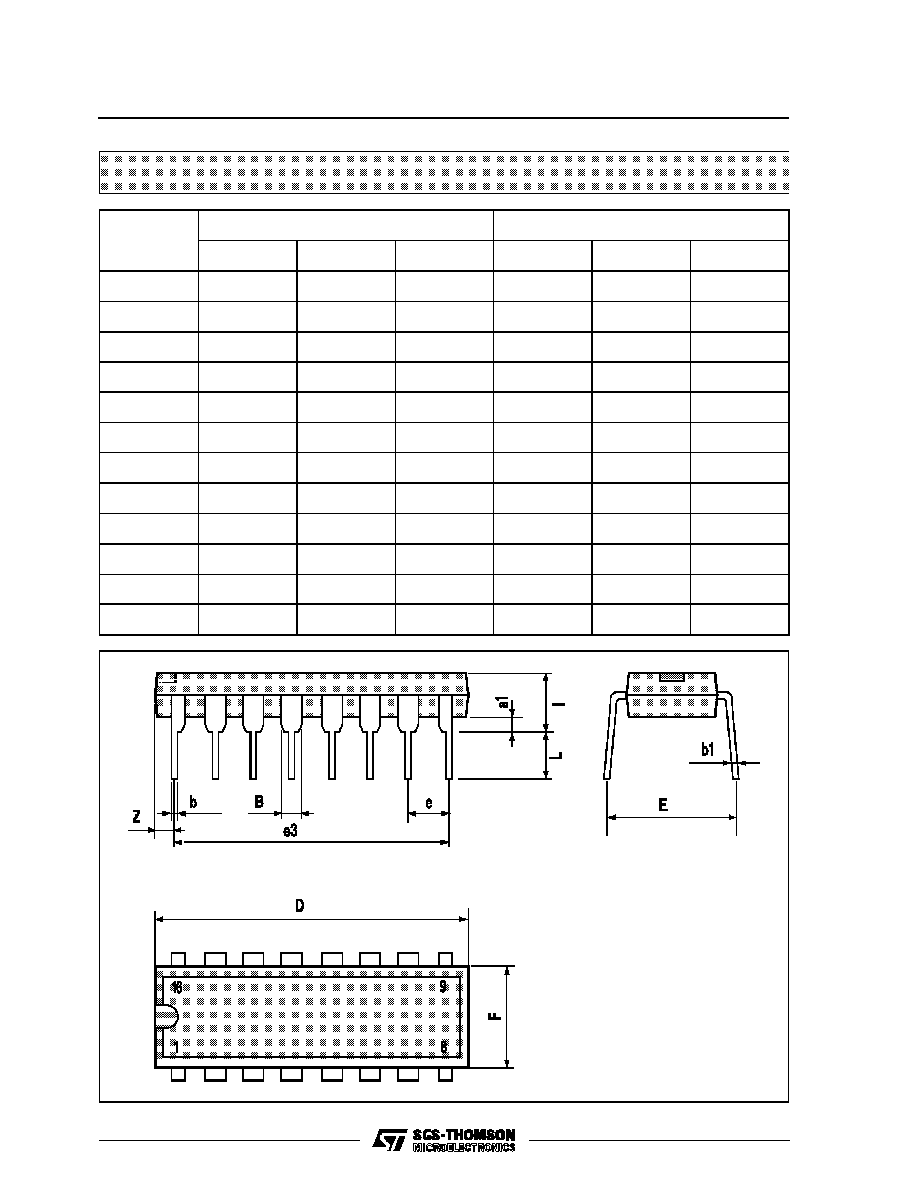
Plastic DIP16 (0.25) MECHANICAL DATA
DIM.
mm
inch
MIN.
TYP.
MAX.
MIN.
TYP.
MAX.
a1
0.51
0.020
B
0.77
1.65
0.030
0.065
b
0.5
0.020
b1
0.25
0.010
D
20
0.787
E
8.5
0.335
e
2.54
0.100
e3
17.78
0.700
F
7.1
0.280
I
5.1
0.201
L
3.3
0.130
Z
1.27
0.050
P001C
M54/M74HC123/123A
10/14
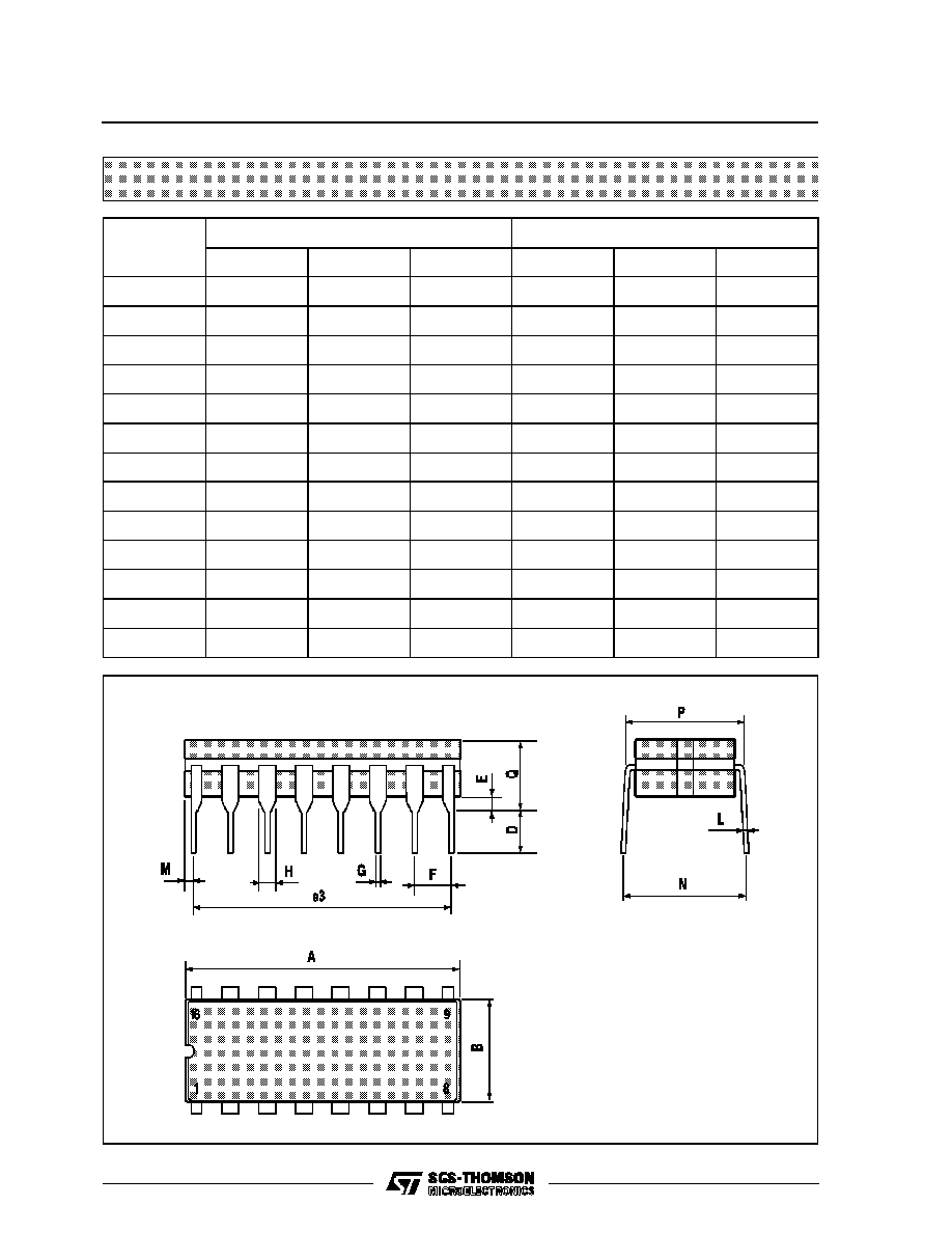
Ceramic DIP16/1 MECHANICAL DATA
DIM.
mm
inch
MIN.
TYP.
MAX.
MIN.
TYP.
MAX.
A
20
0.787
B
7
0.276
D
3.3
0.130
E
0.38
0.015
e3
17.78
0.700
F
2.29
2.79
0.090
0.110
G
0.4
0.55
0.016
0.022
H
1.17
1.52
0.046
0.060
L
0.22
0.31
0.009
0.012
M
0.51
1.27
0.020
0.050
N
10.3
0.406
P
7.8
8.05
0.307
0.317
Q
5.08
0.200
P053D
M54/M74HC123/123A
11/14
SO16 (Narrow) MECHANICAL DATA
DIM.
mm
inch
MIN.
TYP.
MAX.
MIN.
TYP.
MAX.
A
1.75
0.068
a1
0.1
0.2
0.004
0.007
a2
1.65
0.064
b
0.35
0.46
0.013
0.018
b1
0.19
0.25
0.007
0.010
C
0.5
0.019
c1
45
∞
(typ.)
D
9.8
10
0.385
0.393
E
5.8
6.2
0.228
0.244
e
1.27
0.050
e3
8.89
0.350
F
3.8
4.0
0.149
0.157
G
4.6
5.3
0.181
0.208
L
0.5
1.27
0.019
0.050
M
0.62
0.024
S
8
∞
(max.)
P013H
M54/M74HC123/123A
12/14
PLCC20 MECHANICAL DATA
DIM.
mm
inch
MIN.
TYP.
MAX.
MIN.
TYP.
MAX.
A
9.78
10.03
0.385
0.395
B
8.89
9.04
0.350
0.356
D
4.2
4.57
0.165
0.180
d1
2.54
0.100
d2
0.56
0.022
E
7.37
8.38
0.290
0.330
e
1.27
0.050
e3
5.08
0.200
F
0.38
0.015
G
0.101
0.004
M
1.27
0.050
M1
1.14
0.045
P027A
M54/M74HC123/123A
13/14

Information furnished is believed to be accurate and reliable. However, SGS-THOMSON Microelectronics assumes no responsability for the
consequences of use of such information nor for any infringement of patents or other rights of third parties which may results from its use. No
license is granted by implication or otherwise under any patent or patent rights of SGS-THOMSON Microelectronics. Specifications mentioned
in this publication are subject to change without notice. This publication supersedes and replaces all information previously supplied.
SGS-THOMSON Microelectronics products are not authorized for use as critical components in life support devices or systems without express
written approval of SGS-THOMSON Microelectonics.
©
1994 SGS-THOMSON Microelectronics - All Rights Reserved
SGS-THOMSON Microelectronics GROUP OF COMPANIES
Australia - Brazil - France - Germany - Hong Kong - Italy - Japan - Korea - Malaysia - Malta - Morocco - The Netherlands -
Singapore - Spain - Sweden - Switzerland - Taiwan - Thailand - United Kingdom - U.S.A
M54/M74HC123/123A
14/14