1/12
July 2001
s
HIGH SPEED :
t
PD
= 23 ns (TYP.) at V
CC
= 6V
s
LOW POWER DISSIPATION:
STAND BY STATE :
I
CC
=4
µ
A (MAX.) at T
A
=25∞C
ACTIVE STATE :
I
CC
=200
µ
A (MAX.) at V
CC
= 5V
s
HIGH NOISE IMMUNITY:
V
NIH
= V
NIL
= 28 % V
CC
(MIN.)
s
SYMMETRICAL OUTPUT IMPEDANCE:
|I
OH
| = I
OL
= 4mA (MIN)
s
BALANCED PROPAGATION DELAYS:
t
PLH
t
PHL
s
WIDE OPERATING VOLTAGE RANGE:
V
CC
(OPR) = 2V to 6V
s
WIDE OUTPUT PULSE WIDTH RANGE :
t
WOUT
= 120 ns ~ 60 s OVER AT V
CC
= 4.5 V
s
PIN AND FUNCTION COMPATIBLE WITH
74 SERIES 123
DESCRIPTION
The M74HC123 is an high speed CMOS
MONOSTABLE MULTIVIBRATOR fabricated with
silicon gate C
2
MOS technology.
There are two trigger inputs, A INPUT (negative
edge) and B INPUT (positive edge). These inputs
are valid for slow rising/falling signals, (tr=tf=l sec).
The device may also be triggered by using the
CLR input (positive-edge) because of the
Schmitt-trigger input; after triggering the output
maintains the MONOSTABLE state for the time
period determined by the external resistor Rx and
capacitor Cx. When Cx > 10nF and Rx > 10K
,
the output pulse width value is approsimatively
given by the formula : tW(OUT) = K
∑
Cx
∑
Rx.
(K
0.45)
.
Taking CLR low breaks this MONOSTABLE
STATE. If the next trigger pulse occurs during the
MONOSTABLE period it makes the
MONOSTABLE period longer. Limit for values of
Cx and Rx : Cx : NO LIMIT
Rx : V
cc
< 3.0V 5K
to 1M
V
cc
> 3.0V 1K
to 1M
All inputs are equipped with protection circuits
against static discharge and transient excess
voltage.
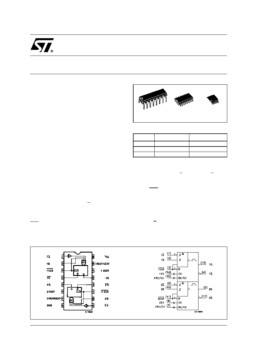
M74HC123
DUAL RETRIGGERABLE MONOSTABLE MULTIVIBRATOR
PIN CONNECTION AND IEC LOGIC SYMBOLS
ORDER CODES
PACKAGE
TUBE
T & R
DIP
M74HC123B1R
SOP
M74HC123M1R
M74HC123RM13TR
TSSOP
M74HC123TTR
TSSOP
DIP
SOP
M74HC123
2/12
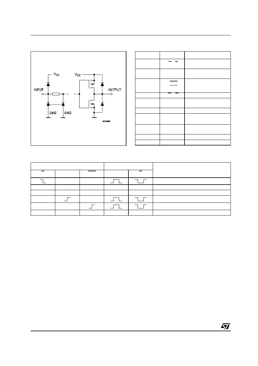
INPUT AND OUTPUT EQUIVALENT CIRCUIT
PIN DESCRIPTION
TRUTH TABLE
X : Don't Care
PIN No
SYMBOL
NAME AND FUNCTION
1,9
1A, 2A
Trigger Inputs (Negative
Edge Triggered)
2, 10
1B, 2B
Trigger Inputs (Positive
Edge Triggered)
3, 11
1 CLR
2 CLR
Direct Reset LOW and
trigger Action at Positive
Edge
4, 12
1Q, 2Q
Outputs (Active Low)
7
2R
X
/C
X
External Resistor
Capacitor Connection
13, 5
1Q, 2Q
Outputs (Active High)
14, 6
1C
X
2C
X
External Capacitor
Connection
15
1R
X
/C
X
External Resistor
Capacitor Connection
8
GND
Ground (0V)
16
Vcc
Positive Supply Voltage
INPUTS
OUTPUTS
NOTE
A
B
CLR
Q
Q
H
H
OUTPUT ENABLE
X
L
H
L
H
INHIBIT
H
X
H
L
H
INHIBIT
L
H
OUTPUT ENABLE
L
H
OUTPUT ENABLE
X
X
L
L
H
INHIBIT

M74HC123
3/12
SYSTEM DIAGRAM
This logic diagram has not be used to estimate propagation delays
TIMING CHART

M74HC123
4/12
BLOCK DIAGRAM
(1) Cx, Rx, Dx are external components.
(2) Dx is a clamping diode.
The external capacitor is charged to Vcc in the stand-by-state, i.e. no trigger. When the supply voltage is turned off Cx is di scharged mainly
trough an internal parasitic diode(see figures). If Cx is sufficiently large and Vcc decreases rapidly, there will be some possibility of damaging
the I.C. with a surge current or latch-up. If the voltage supply filter capacitor is large enough and Vcc decrease slowly, the surge current is
automatically limited and damage to the I.C. is avoided. The maximum forward current of the parasitic diode is approximately 20 mA. In cases
where Cx is large the time taken for the supply voltage to fall to 0.4 Vcc can be calculated as follows :
t
f
> (Vcc - 0.7) x Cx/20mA
In cases where t
f
is too short an external clamping diode is required to protect the I.C. from the surge current.
FUNCTIONAL DESCRIPTION
STAND-BY STATE
The external capacitor,Cx, is fully charged to Vcc
in the stand-by state. Hence, before triggering,
transistor Qp and Qn (connected to the Rx/Cx
node) are both turned-off. The two comparators
that control the timing and the two reference
voltage sources stop operating. The total supply
current is therefore only leakage current.
TRIGGER OPERATION
Triggering occurs when :
1 st) A is "LOW" and B has a falling edge;
2 nd) B is "HIGH" and A has a rising edge;
3 rd) A is "LOW" and B is HIGH and C1 has a
rising edge;
After the multivibrator has been retriggered
comparator C1 and C2 start operating and Qn is
turned on. Cx then discharges through Qn. The
voltage at the node R/C external falls.
When it reaches V
REFL
the output of comparator
C1 becomes low. This in turn reset the flip-flop
and Qn is turned off.
At this point C1 stops functioning but C2 continues
to operate.
The voltage at R/C external begins to rise with a
time constant set by the external components Rx,
Cx.
Triggering the multivibrator causes Q to go high
after internal delay due to the flip-flop and the
gate. Q remains high until the voltage at R/C
external rises again to V
REFH
. At this point C2
output goes low and O goes low. C2 stop
operating. That means that after triggering when
the voltage R/C external returns to V
REFH
the
multivibrator has returned to its MONOSTABLE
STATE. In the case where Rx ∑ Cx are large
enough and the discharge time of the capacitor
and the delay time in the I.C. can be ignored, the
width of the output pulse tw (out) is as follows :
tW(OUT) = 0.45 Cx ∑ Rx
RE - TRIGGERED OPERATION
When a second trigger pulse follows the first its
effect will depend on the state of the multivibrator.
If the capacitor Cx is being charged the voltage
level of R/C external falls to V
REFL
again and Q
remains High i.e. the retrigger pulse arrives in a
time shorter than the period Rx ∑ Cx seconds, the
capacitor charging time constant. If the second
trigger pulse is very close to the initial trigger pulse
it is ineffective ; i.e. the second trigger must arrive
in the capacitor discharge cycle to be ineffective;
Hence the minimum time for a second trigger to be
effective depends on Vcc and Cx
RESET OPERATION
CL is normally high. If CL is low, the trigger is not
effective because Q output goes low and trigger
control flip-flop is reset.
Also transistor Op is turned on and Cx is charged
quickly to Vcc. This means if CL input goes low the
IC becomes waiting state both in operating and
non operating state.
M74HC123
5/12
ABSOLUTE MAXIMUM RATINGS
Absolute Maximum Ratings are those values beyond which damage to the device may occur. Functional operation under these conditions is
not implied
(*) 500mW at 65
∞
C; derate to 300mW by 10mW/
∞
C from 65
∞
C to 85
∞
C
RECOMMENDED OPERATING CONDITIONS
The Maximum allowable values of Cx and Rx are a function of leakage of capacitor Cx, the leakage of device and leakage due to the board
layout and surface resistance. Susceptibility to externally induced noise may occur for Rx > 1M
Symbol
Parameter
Value
Unit
V
CC
Supply Voltage
-0.5 to +7
V
V
I
DC Input Voltage
-0.5 to V
CC
+ 0.5
V
V
O
DC Output Voltage
-0.5 to V
CC
+ 0.5
V
I
IK
DC Input Diode Current
±
20
mA
I
OK
DC Output Diode Current
±
20
mA
I
O
DC Output Current
±
25
mA
I
CC
or I
GND
DC V
CC
or Ground Current
±
50
mA
P
D
Power Dissipation
500(*)
mW
T
stg
Storage Temperature
-65 to +150
∞C
T
L
Lead Temperature (10 sec)
300
∞C
Symbol
Parameter
Value
Unit
V
CC
Supply Voltage
2 to 6
V
V
I
Input Voltage
0 to V
CC
V
V
O
Output Voltage
0 to V
CC
V
T
op
Operating Temperature
-55 to 125
∞C
t
r
, t
f
Input Rise and Fall Time
V
CC
= 2.0V
0 to 1000
ns
V
CC
= 4.5V
0 to 500
ns
V
CC
= 6.0V
0 to 400
ns
Cx
External Capacitor
NO LIMITATION
pF
Rx
External Resistor
Vcc < 3V
5K to 1M
Vcc > 3V
1K to 1M