1/12
July 2001
s
HIGH SPEED:
t
PD
= 17ns (TYP.) at V
CC
= 6V
s
LOW POWER DISSIPATION:
I
CC
= 4
µ
A(MAX.) at T
A
=25∞C
s
HIGH NOISE IMMUNITY:
V
NIH
= V
NIL
= 28 % V
CC
(MIN.)
s
SYMMETRICAL OUTPUT IMPEDANCE:
|I
OH
| = I
OL
= 4mA (MIN)
s
BALANCED PROPAGATION DELAYS:
t
PLH
t
PHL
s
WIDE OPERATING VOLTAGE RANGE:
V
CC
(OPR) = 2V to 6V
s
PIN AND FUNCTION COMPATIBLE WITH
74 SERIES 151
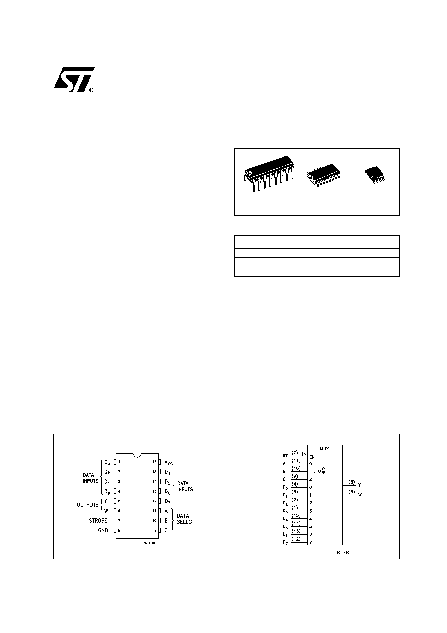
DESCRIPTION
The M74HC151 is an high speed CMOS 8
CHANNEL MULTIPLEXER fabricated with silicon
gate C
2
MOS technology.
It provides, in one package, the ability to select
one bit of data from up to eight sources. The
M74HC151 can be used as a universal function
generator to generate any logic function of four
variables. Outputs Y and W are complementary;
the selection depends on the address inputs A, B,
and C. The strobe input must be taken low to
enable this device, when the strobe is high W
output is forced high and consequently Y output
goes low. All inputs are equipped with protection
circuits against static discharge and transient
excess voltage.
M74HC151
8 CHANNEL MULTIPLEXER
PIN CONNECTION AND IEC LOGIC SYMBOLS
ORDER CODES
PACKAGE
TUBE
T & R
DIP
M74HC151B1R
SOP
M74HC151M1R
M74HC151RM13TR
TSSOP
M74HC151TTR
TSSOP
DIP
SOP
M74HC151
4/12
ABSOLUTE MAXIMUM RATINGS
Absolute Maximum Ratings are those values beyond which damage to the device may occur. Functional operation under these conditions is
not implied
(*) 500mW at 65
∞
C; derate to 300mW by 10mW/
∞
C from 65
∞
C to 85
∞
C
RECOMMENDED OPERATING CONDITIONS
Symbol
Parameter
Value
Unit
V
CC
Supply Voltage
-0.5 to +7
V
V
I
DC Input Voltage
-0.5 to V
CC
+ 0.5
V
V
O
DC Output Voltage
-0.5 to V
CC
+ 0.5
V
I
IK
DC Input Diode Current
±
20
mA
I
OK
DC Output Diode Current
±
20
mA
I
O
DC Output Current
±
25
mA
I
CC
or I
GND
DC V
CC
or Ground Current
±
50
mA
P
D
Power Dissipation
500(*)
mW
T
stg
Storage Temperature
-65 to +150
∞C
T
L
Lead Temperature (10 sec)
300
∞C
Symbol
Parameter
Value
Unit
V
CC
Supply Voltage
2 to 6
V
V
I
Input Voltage
0 to V
CC
V
V
O
Output Voltage
0 to V
CC
V
T
op
Operating Temperature
-55 to 125
∞C
t
r
, t
f
Input Rise and Fall Time
V
CC
= 2.0V
0 to 1000
ns
V
CC
= 4.5V
0 to 500
ns
V
CC
= 6.0V
0 to 400
ns


