
1/13
June 2003
s
HIGH SPEED :
f
MAX
= 62MHz (TYP.) at V
CC
= 6V
s
LOW POWER DISSIPATION:
I
CC
=4
µ
A(MAX.) at T
A
=25∞C
s
HIGH NOISE IMMUNITY:
V
NIH
= V
NIL
= 28 % V
CC
(MIN.)
s
SYMMETRICAL OUTPUT IMPEDANCE:
|I
OH
| = I
OL
= 4mA (MIN)
s
BALANCED PROPAGATION DELAYS:
t
PLH
t
PHL
s
WIDE OPERATING VOLTAGE RANGE:
V
CC
(OPR) = 2V to 6V
s
PIN AND FUNCTION COMPATIBLE WITH
74 SERIES 164
DESCRIPTION
The M74HC164 is an high speed CMOS 8 BIT
SIPO SHIFT REGISTER fabricated with silicon
gate C
2
MOS technology.
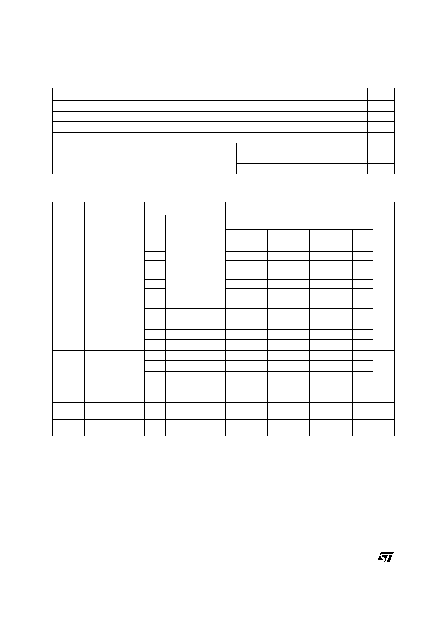
The M74HC164 is an 8 bit shift register with serial
data entry and an output from each of the eight
stages. Data is entered serially through one of two
inputs (A or B), either of these inputs can be used
as an active high enable for data entry through the
other input. An unused input must be high, or both
inputs connected together. Each low-to-high
transition on the clock inputs shifts data one place
to the right and enters into QA the logic NAND of
the two data inputs (A x B), the data that existed
before the rising clock edge. A low level on the
clear input overrides all other inputs and clears the
register asynchronously, forcing all Q outputs low.
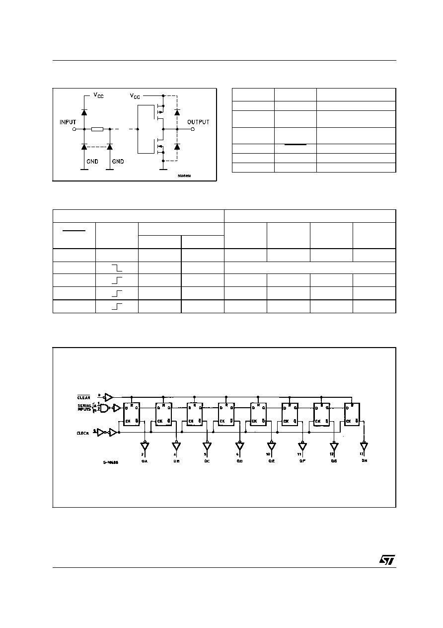
All inputs are equipped with protection circuits
against static discharge and transient excess
voltage.
M74HC164
8 BIT SIPO SHIFT REGISTER
PIN CONNECTION AND IEC LOGIC SYMBOLS
ORDER CODES
PACKAGE
TUBE
T & R
DIP
M74HC164B1R
SOP
M74HC164M1R
M74HC164RM13TR
TSSOP
M74HC164TTR
TSSOP
DIP
SOP
M74HC164
2/13
INPUT AND OUTPUT EQUIVALENT CIRCUIT
PIN DESCRIPTION
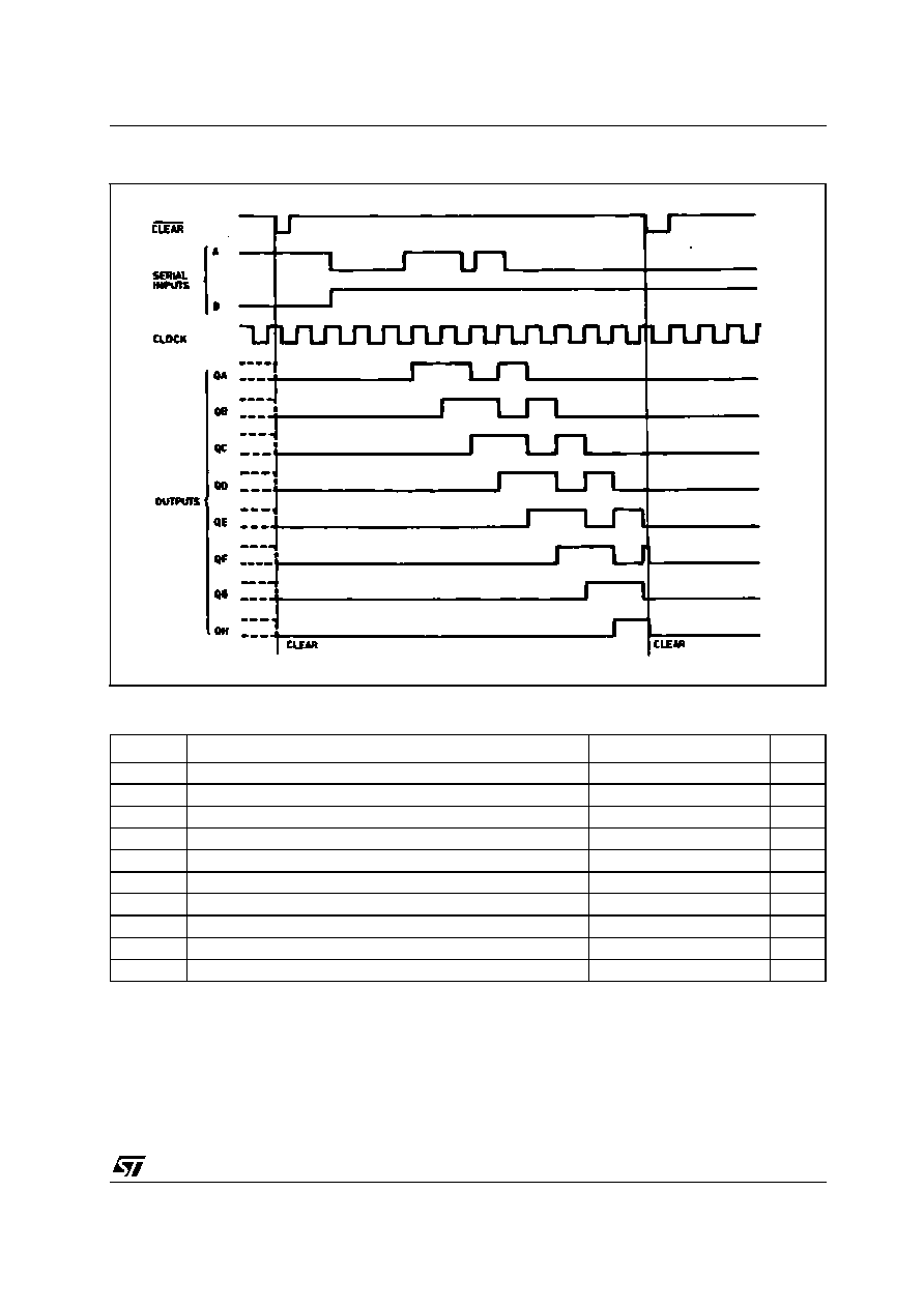
TRUTH TABLE
X : Don't Care
QAn - QGn : The level of QA - QG, respectively. before the most-recent transition of the clock
LOGIC DIAGRAM
This logic diagram has not be used to estimate propagation delays
PIN No
SYMBOL
NAME AND FUNCTION
1,2
A, B
Data Inputs
3, 4, 5, 6, 10,
11, 12, 13
QA to QH
Outputs
8
CLOCK
Clock Input (LOW to
HIGH, Edge Triggered
9
CLEAR
Master Reset Input
7
GND
Ground (0V)
14
Vcc
Positive Supply Voltage
INPUTS
OUTPUTS
CLEAR
CLOCK
SERIAL IN
QA
QB
...........
QH
A
B
L
X
X
X
L
L
...........
L
H
X
X
NO CHANGE
H
L
X
L
QAn
...........
QGn
H
X
L
L
QAn
...........
QGn
H
H
H
H
QAn
...........
QGn
M74HC164
3/13
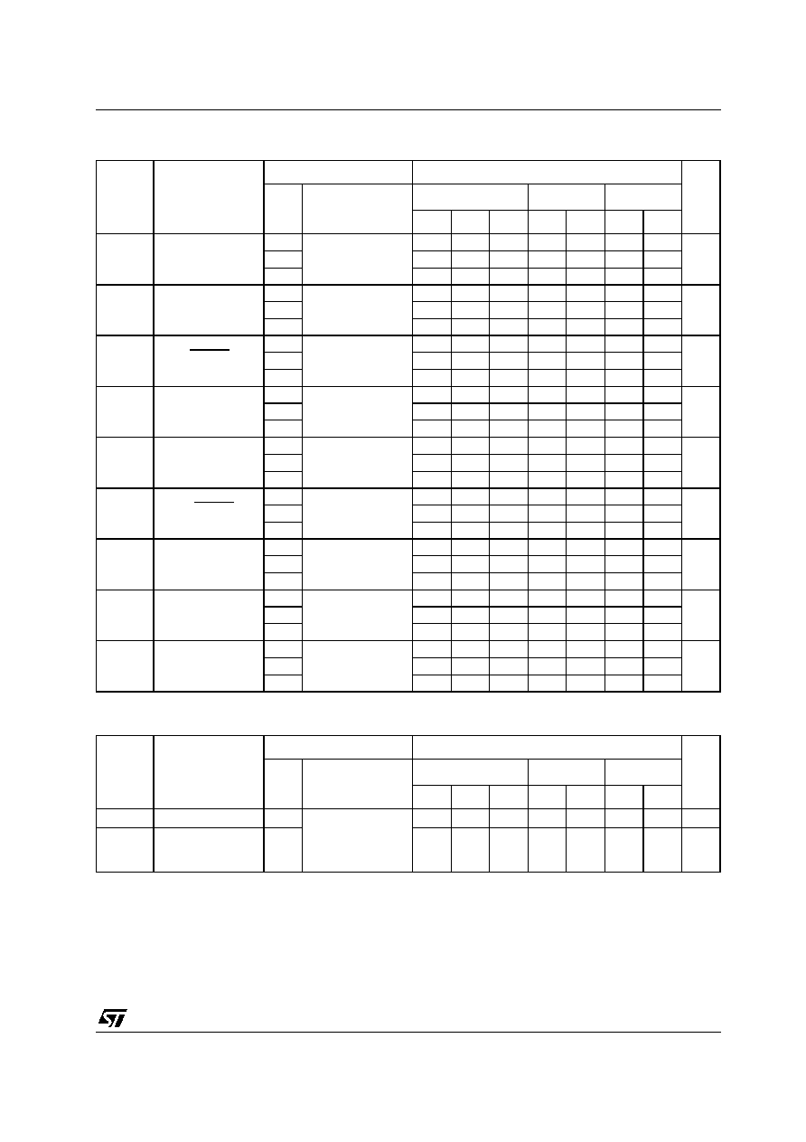
TIMING CHART
ABSOLUTE MAXIMUM RATINGS
Absolute Maximum Ratings are those values beyond which damage to the device may occur. Functional operation under these conditions is
not implied
(*) 500mW at 65
∞
C; derate to 300mW by 10mW/
∞
C from 65
∞
C to 85
∞
C
Symbol
Parameter
Value
Unit
V
CC
Supply Voltage
-0.5 to +7
V
V
I
DC Input Voltage
-0.5 to V
CC
+ 0.5
V
V
O
DC Output Voltage
-0.5 to V
CC
+ 0.5
V
I
IK
DC Input Diode Current
±
20
mA
I
OK
DC Output Diode Current
±
20
mA
I
O
DC Output Current
±
25
mA
I
CC
or I
GND
DC V
CC
or Ground Current
±
50
mA
P
D
Power Dissipation
500(*)
mW
T
stg
Storage Temperature
-65 to +150
∞C
T
L
Lead Temperature (10 sec)
300
∞C
M74HC164
4/13
RECOMMENDED OPERATING CONDITIONS
DC SPECIFICATIONS
Symbol
Parameter
Value
Unit
V
CC
Supply Voltage
2 to 6
V
V
I
Input Voltage
0 to V
CC
V
V
O
Output Voltage
0 to V
CC
V
T
op
Operating Temperature
-55 to 125
∞C
t
r
, t
f
Input Rise and Fall Time
V
CC
= 2.0V
0 to 1000
ns
V
CC
= 4.5V
0 to 500
ns
V
CC
= 6.0V
0 to 400
ns
Symbol
Parameter
Test Condition
Value
Unit
V
CC
(V)
T
A
= 25∞C
-40 to 85∞C
-55 to 125∞C
Min.
Typ.
Max.
Min.
Max.
Min.
Max.
V
IH
High Level Input
Voltage
2.0
1.5
1.5
1.5
V
4.5
3.15
3.15
3.15
6.0
4.2
4.2
4.2
V
IL
Low Level Input
Voltage
2.0
0.5
0.5
0.5
V
4.5
1.35
1.35
1.35
6.0
1.8
1.8
1.8
V
OH
High Level Output
Voltage
2.0
I
O
=-20
µ
A
1.9
2.0
1.9
1.9
V
4.5
I
O
=-20
µ
A
4.4
4.5
4.4
4.4
6.0
I
O
=-20
µ
A
5.9
6.0
5.9
5.9
4.5
I
O
=-4.0 mA
4.18
4.31
4.13
4.10
6.0
I
O
=-5.2 mA
5.68
5.8
5.63
5.60
V
OL
Low Level Output
Voltage
2.0
I
O
=20
µ
A
0.0
0.1
0.1
0.1
V
4.5
I
O
=20
µ
A
0.0
0.1
0.1
0.1
6.0
I
O
=20
µ
A
0.0
0.1
0.1
0.1
4.5
I
O
=4.0 mA
0.17
0.26
0.33
0.40
6.0
I
O
=5.2 mA
0.18
0.26
0.33
0.40
I
I
Input Leakage
Current
6.0
V
I
= V
CC
or GND
±
0.1
±
1
±
1
µ
A
I
CC
Quiescent Supply
Current
6.0
V
I
= V
CC
or GND
4
40
80
µ
A
M74HC164
5/13
AC ELECTRICAL CHARACTERISTICS (C
L
= 50 pF, Input t
r
= t
f
= 6ns)
CAPACITIVE CHARACTERISTICS
1) C
PD
is defined as the value of the IC's internal equivalent capacitance which is calculated from the operating current consumption without
load. (Refer to Test Circuit). Average operating current can be obtained by the following equation. I
CC(opr)
= C
PD
x V
CC
x f
IN
+ I
CC
Symbol
Parameter
Test Condition
Value
Unit
V
CC
(V)
T
A
= 25∞C
-40 to 85∞C
-55 to 125∞C
Min.
Typ.
Max.
Min.
Max.
Min.
Max.
t
TLH
t
THL
Output Transition
Time
2.0
30
75
95
110
ns
4.5
8
15
19
22
6.0
7
13
16
19
t
PLH
t
PHL
Propagation Delay
Time (CLOCK - Q)
2.0
57
160
200
240
ns
4.5
19
32
40
48
6.0
16
27
34
41
t
PLH
t
PHL
Propagation Delay
Time (CLEAR - Q)
2.0
60
175
220
265
ns
4.5
20
35
44
53
6.0
17
30
37
45
f
MAX
Maximum Clock
Frequency
2.0
6.2
18
5.0
4.2
MHz
4.5
31
53
25
21
6.0
37
62
30
25
t
W(H)
t
W(L)
Minimum Pulse
Width (CLOCK)
2.0
24
75
95
110
ns
4.5
6
15
19
22
6.0
5
13
16
19
t
W(L)
Minimum Pulse
Width (CLEAR)
2.0
40
75
95
110
ns
4.5
10
15
19
22
6.0
9
13
16
19
t
s
Set-up Time (A, B -
CK)
2.0
50
65
75
ns
4.5
10
13
15
6.0
9
11
13
t
h
Hold Time (A, B -
CK)
2.0
5
5
5
ns
4.5
5
5
5
6.0
5
5
5
t
REM
Minimum Removal
Time
2.0
5
5
5
ns
4.5
5
5
5
6.0
5
5
5
Symbol
Parameter
Test Condition
Value
Unit
V
CC
(V)
T
A
= 25∞C
-40 to 85∞C
-55 to 125∞C
Min.
Typ.
Max.
Min.
Max.
Min.
Max.
C
IN
Input Capacitance
5.0
5
10
10
10
pF
C
PD
Power Dissipation
Capacitance (note
1)
5.0
99
pF