
M54HC166
M74HC166
October 1992
8 BIT PISO SHIFT REGISTER
B1R
(Plastic Package)
ORDER CODES :
M54HC166F1R
M74HC166M1R
M74HC166B1R
M74HC166C1R
F1R
(Ceramic Package)
M1R
(Micro Package)
C1R
(Chip Carrier)
PIN CONNECTIONS (top view)
NC =
No Inter-
nal Con-
DESCRIPTION
.
HIGH SPEED
f
MAX
= 57 MHz (TYP.) AT V
CC
= 5 V
.
LOW POWER DISSIPATION
I
CC
= 4
µ
A (MAX.) AT T
A
= 25
∞
C
.
HIGH NOISE IMMUNITY
V
NIH
= V
NIL
= 28 % V
CC
(MIN.)
.
OUTPUT DRIVE CAPABILITY
10 LSTTL LOADS
.
SYMMETRICAL OUTPUT IMPEDANCE
|I
OH
| = I
OL
= 4 mA (MIN.)
.
BALANCED PROPAGATION DELAYS
t
PLH
= t
PHL
.
WIDE OPERATING VOLTAGE RANGE
V
CC
(OPR) = 2 V TO 6 V
.
PIN AND FUNCTION COMPATIBLE WITH
54/74LS166
The M54/74HC166 is a high speed C
2
MOS 8 BIT
PISO SHIFT REGISTER fabricated in silicon gate
C
2
MOS technology. It has the same high speed per-
formance of LSTTL combined with true CMOS low
power consumption.
It consists of parallel or serial inputs and a serial-out
8-bit shift register with gated clock inputs and an
overriding clear input. The parallel-in or serial-in
modes are controlled by the SHIFT/LOAD input.
When the SHIFT/LOAD input is held high, the serial
data input is enabled and the eight flip-flops perform
serial shifting with each clock pulse. When held low,
the parallel data inputs are enabled and syn-
chronous loading occurs on the next clock pulse.
Clocking is accomplished on the low-to-high level
edge of the clock pulse. The CLOCK-INHIBIT input
should be changed to the high only while the
CLOCK input is held high. A direct clear input over-
rides all other inputs, including the clock, and sets
all flip-flops to zero. Functional details are shown in
the truth table and the timing chart.
All inputs are equipped with protection circuits
against static discharge and transient excess volt-
age.
1/13
PIN DESCRIPTION
PIN No
SYMBOL
NAME AND FUNCTION
1
SI
Serial Data Inputs
2, 3, 4, 5,
10, 11, 12,
14
A to H
Parallel Data Inputs
6
CK INH
Clock Enable Input
(Active LOW)
7
CK
Clock Input (LOW to
HIGH edge-triggered)
9
CLEAR
Asyncronous Master reset
Input (Active LOW)
13
Q
H
Serial Output from the
Last Stage
15
S/L
Parallel Enable Input
(Active LOW)
8
GND
Ground (0V)
16
V
CC
Positive Supply Voltage
IEC LOGIC SYMBOL
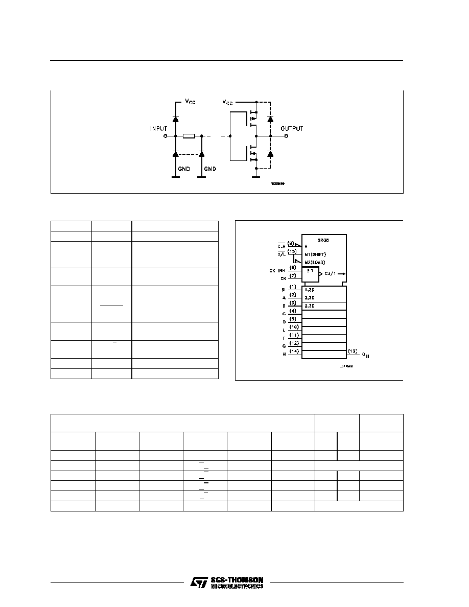
INPUT AND OUTPUT EQUIVALENT CIRCUIT
TRUTH TABLE
INPUTS
INTERNAL
OUTPUTS
OUTPUTS
CLEAR
SHIFT/LOAD CLOCK INH
CLOCK
SERIAL IN
PARALLEL
A...............H
QA
QB
QH
L
X
X
X
X
X
L
L
L
L
X
X
X
X
NO CHANGE
H
L
L
X
a................h
a
b
h
H
H
L
H
X
H
QAn
QGn
H
H
L
L
X
L
QAn
QGn
H
X
H
X
X
X
NO CHANGE
X: Don't Care
a...........h : The level of steady state input voltage at inputs a trough H respectively
M54/M74HC166
2/13
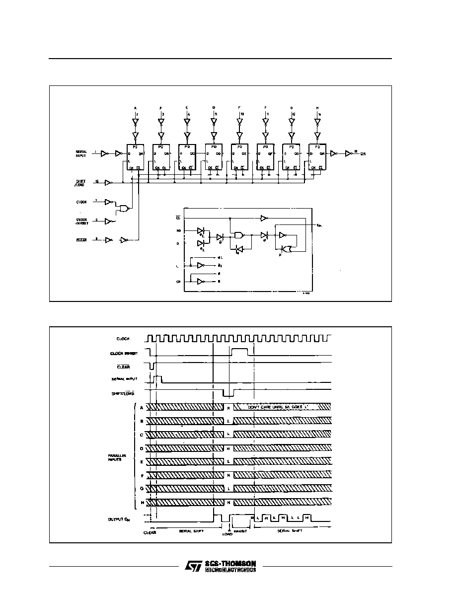
LOGIC DIAGRAM
TIMING CHART
PARALLEL INPUTS
M54/M74HC166
3/13

ABSOLUTE MAXIMUM RATINGS
Symbol
Parameter
Value
Unit
V
CC
Supply Voltage
-0.5 to +7
V
V
I
DC Input Voltage
-0.5 to V
CC
+ 0.5
V
V
O
DC Output Voltage
-0.5 to V
CC
+ 0.5
V
I
IK
DC Input Diode Current
±
20
mA
I
OK
DC Output Diode Current
±
20
mA
I
O
DC Output Source Sink Current Per Output Pin
±
25
mA
I
CC
or I
GND
DC V
CC
or Ground Current
±
50
mA
P
D
Power Dissipation
500 (*)
mW
T
stg
Storage Temperature
-65 to +150
o
C
T
L
Lead Temperature (10 sec)
300
o
C
Absolute Maximum Ratings are those values beyond which damage to the device may occur. Functional operation under these condition is not implied.
(*) 500 mW:
65
o
C derate to 300 mW by 10mW/
o
C: 65
o
C to 85
o
C
RECOMMENDED OPERATING CONDITIONS
Symbol
Parameter
Value
Unit
V
CC
Supply Voltage
2 to 6
V
V
I
Input Voltage
0 to V
CC
V
V
O
Output Voltage
0 to V
CC
V
T
op
Operating Temperature: M54HC Series
M74HC Series
-55 to +125
-40 to +85
o
C
o
C
t
r
, t
f
Input Rise and Fall Time
V
CC
= 2 V
0 to 1000
ns
V
CC
= 4.5 V
0 to 500
V
CC
= 6 V
0 to 400
M54/M74HC166
4/13

DC SPECIFICATIONS
Symbol
Parameter
Test Conditions
Value
Unit
V
CC
(V)
T
A
= 25
o
C
54HC and 74HC
-40 to 85
o
C
74HC
-55 to 125
o
C
54HC
Min.
Typ.
Max.
Min.
Max.
Min.
Max.
V
IH
High Level Input
Voltage
2.0
1.5
1.5
1.5
V
4.5
3.15
3.15
3.15
6.0
4.2
4.2
4.2
V
IL
Low Level Input
Voltage
2.0
0.5
0.5
0.5
V
4.5
1.35
1.35
1.35
6.0
1.8
1.8
1.8
V
OH
High Level
Output Voltage
2.0
V
I
=
V
IH
or
V
IL
I
O
=-20
µ
A
1.9
2.0
1.9
1.9
V
4.5
4.4
4.5
4.4
4.4
6.0
5.9
6.0
5.9
5.9
4.5
I
O
=-4.0 mA
4.18
4.31
4.13
4.10
6.0
I
O
=-5.2 mA
5.68
5.8
5.63
5.60
V
OL
Low Level Output
Voltage
2.0
V
I
=
V
IH
or
V
IL
I
O
= 20
µ
A
0.0
0.1
0.1
0.1
V
4.5
0.0
0.1
0.1
0.1
6.0
0.0
0.1
0.1
0.1
4.5
I
O
= 4.0 mA
0.17
0.26
0.33
0.40
6.0
I
O
= 5.2 mA
0.18
0.26
0.33
0.40
I
I
Input Leakage
Current
6.0
V
I
= V
CC
or GND
±
0.1
±
1
±
1
µ
A
I
CC
Quiescent Supply
Current
6.0
V
I
= V
CC
or GND
4
40
80
µ
A
M54/M74HC166
5/13
AC ELECTRICAL CHARACTERISTICS (C
L
= 50 pF, Input t
r
= t
f
= 6 ns)
Symbol
Parameter
Test Conditions
Value
Unit
V
CC
(V)
T
A
= 25
o
C
54HC and 74HC
-40 to 85
o
C
74HC
-55 to 125
o
C
54HC
Min.
Typ.
Max.
Min.
Max.
Min.
Max.
t
TLH
t
THL
Output Transition
Time
2.0
30
75
95
110
ns
4.5
8
15
19
22
6.0
7
13
16
19
t
PLH
t
PHL
Propagation
Delay Time
(CLOCK - QH)
2.0
70
150
190
225
ns
4.5
20
30
38
45
6.0
16
26
32
38
t
PHL
Propagation
Delay Time
(CLEAR - QH)
2.0
60
135
170
205
ns
4.5
18
27
34
41
6.0
14
23
29
35
f
MAX
Maximum Clock
Frequency
2.0
6.2
14
5.0
4.2
MHz
4.5
31
50
25
21
6.0
37
63
30
25
t
W(H)
t
W(L)
Minimum Pulse
Width
(CLOCK)
2.0
28
75
95
110
ns
4.5
6
15
19
22
6.0
5
13
16
19
t
W(L)
Minimum Pulse
Width
(CLEAR)
2.0
28
75
95
110
ns
4.5
6
15
19
22
6.0
5
13
16
19
t
s
Minimum Set-up
Time
(SI, PI)
2.0
20
75
95
110
ns
4.5
4
15
19
22
6.0
3
13
16
19
t
s
Minimum Set-up
Time
(S/L)
2.0
25
75
95
110
ns
4.5
5
15
19
22
6.0
3
13
16
19
t
h
Minimum Hold
Time
2.0
0
0
0
ns
4.5
0
0
0
6.0
0
0
0
t
REM
Minimum
Removal Time
2.0
12
50
65
75
ns
4.5
3
10
13
15
6.0
3
9
11
13
C
IN
Input Capacitance
5
10
10
10
pF
C
PD
(*)
Power Dissipation
Capacitance
60
pF
(*) C
PD
is defined as the value of the IC's internal equivalent capacitance which is calculated from the operating current consumption without load.
(Refer to Test Circuit). Average operting current can be obtained by the following equation. I
CC
(opr) = C
PD
∑
V
CC
∑
f
IN
+ I
CC
M54/M74HC166
6/13
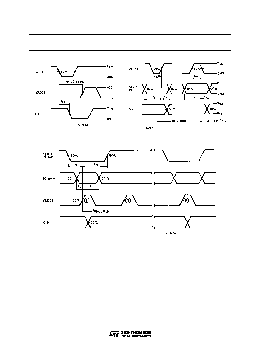
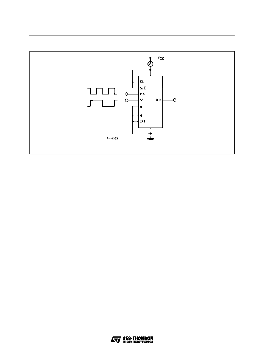
SWITCHING CHARACTERISTICS TEST WAVEFORM
CLEAR MODE
SERIAL MODE
PARALLEL MODE
M54/M74HC166
7/13
TEST CIRCUIT I
CC
(Opr.)
INPUT WAVEFORM IS THE SAME AS THAT IN CASE OF SWITCHING CHARACTERISTICS TEST.
M54/M74HC166
8/13

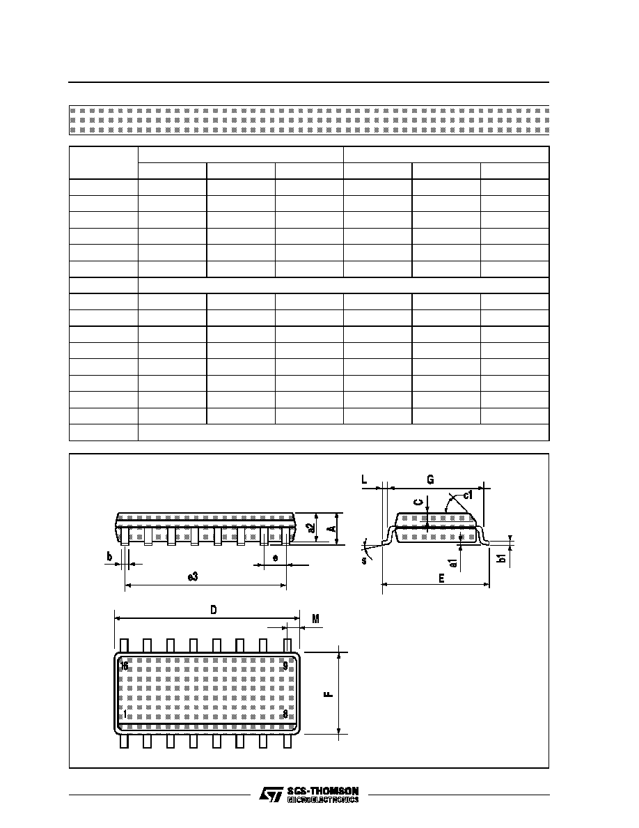
Plastic DIP16 (0.25) MECHANICAL DATA
DIM.
mm
inch
MIN.
TYP.
MAX.
MIN.
TYP.
MAX.
a1
0.51
0.020
B
0.77
1.65
0.030
0.065
b
0.5
0.020
b1
0.25
0.010
D
20
0.787
E
8.5
0.335
e
2.54
0.100
e3
17.78
0.700
F
7.1
0.280
I
5.1
0.201
L
3.3
0.130
Z
1.27
0.050
P001C
M54/M74HC166
9/13

Ceramic DIP16/1 MECHANICAL DATA
DIM.
mm
inch
MIN.
TYP.
MAX.
MIN.
TYP.
MAX.
A
20
0.787
B
7
0.276
D
3.3
0.130
E
0.38
0.015
e3
17.78
0.700
F
2.29
2.79
0.090
0.110
G
0.4
0.55
0.016
0.022
H
1.17
1.52
0.046
0.060
L
0.22
0.31
0.009
0.012
M
0.51
1.27
0.020
0.050
N
10.3
0.406
P
7.8
8.05
0.307
0.317
Q
5.08
0.200
P053D
M54/M74HC166
10/13
SO16 (Narrow) MECHANICAL DATA
DIM.
mm
inch
MIN.
TYP.
MAX.
MIN.
TYP.
MAX.
A
1.75
0.068
a1
0.1
0.2
0.004
0.007
a2
1.65
0.064
b
0.35
0.46
0.013
0.018
b1
0.19
0.25
0.007
0.010
C
0.5
0.019
c1
45
∞
(typ.)
D
9.8
10
0.385
0.393
E
5.8
6.2
0.228
0.244
e
1.27
0.050
e3
8.89
0.350
F
3.8
4.0
0.149
0.157
G
4.6
5.3
0.181
0.208
L
0.5
1.27
0.019
0.050
M
0.62
0.024
S
8
∞
(max.)
P013H
M54/M74HC166
11/13
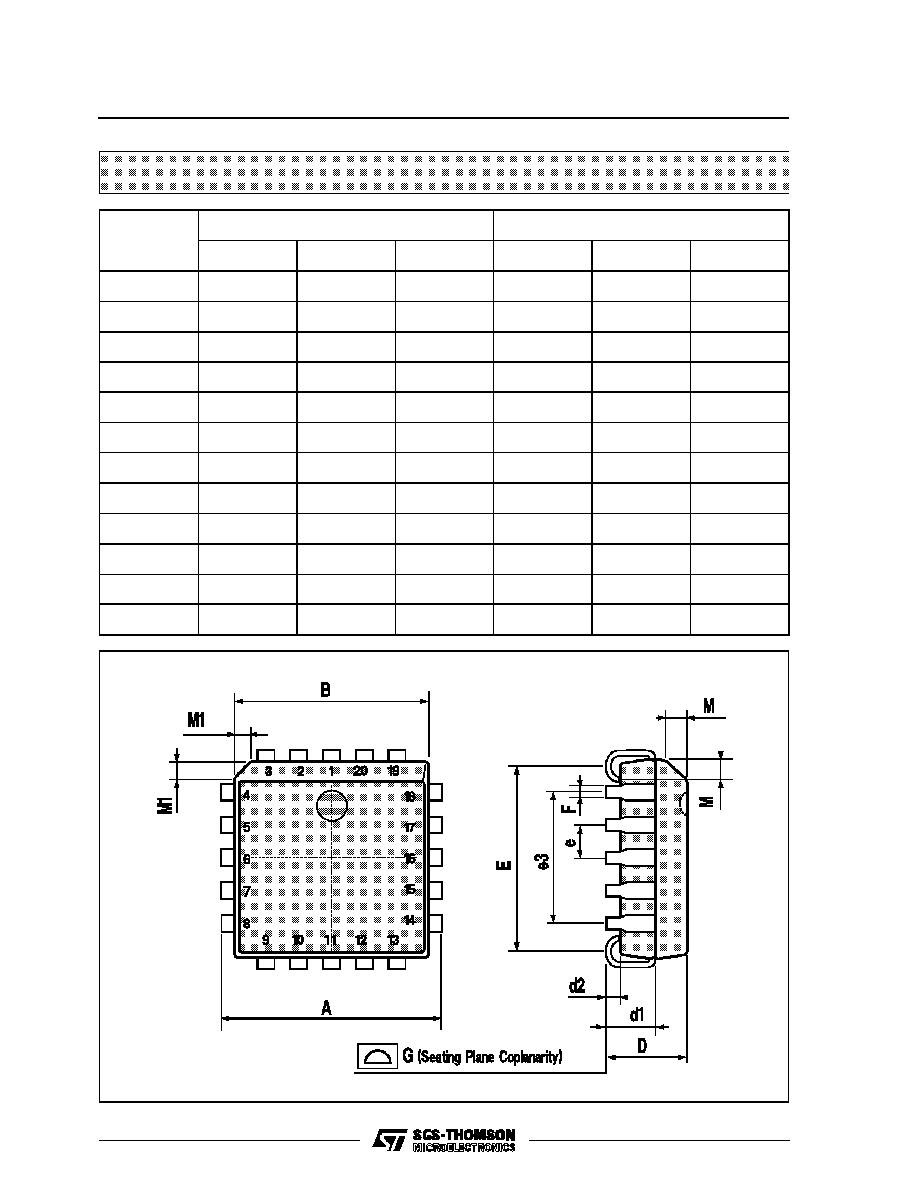
PLCC20 MECHANICAL DATA
DIM.
mm
inch
MIN.
TYP.
MAX.
MIN.
TYP.
MAX.
A
9.78
10.03
0.385
0.395
B
8.89
9.04
0.350
0.356
D
4.2
4.57
0.165
0.180
d1
2.54
0.100
d2
0.56
0.022
E
7.37
8.38
0.290
0.330
e
1.27
0.050
e3
5.08
0.200
F
0.38
0.015
G
0.101
0.004
M
1.27
0.050
M1
1.14
0.045
P027A
M54/M74HC166
12/13

Information furnished is believed to be accurate and reliable. However, SGS-THOMSON Microelectronics assumes no responsability for the
consequences of use of such information nor for any infringement of patents or other rights of third parties which may results from its use. No
license is granted by implication or otherwise under any patent or patent rights of SGS-THOMSON Microelectronics. Specifications mentioned
in this publication are subject to change without notice. This publication supersedes and replaces all information previously supplied.
SGS-THOMSON Microelectronics products are not authorized for use as critical components in life support devices or systems without express
written approval of SGS-THOMSON Microelectonics.
©
1994 SGS-THOMSON Microelectronics - All Rights Reserved
SGS-THOMSON Microelectronics GROUP OF COMPANIES
Australia - Brazil - France - Germany - Hong Kong - Italy - Japan - Korea - Malaysia - Malta - Morocco - The Netherlands -
Singapore - Spain - Sweden - Switzerland - Taiwan - Thailand - United Kingdom - U.S.A
M54/M74HC166
13/13