
1/12
July 2001
s
HIGH SPEED :
f
MAX
= 63 MHz (TYP.) at V
CC
= 6V
s
LOW POWER DISSIPATION:
I
CC
=4
µ
A(MAX.) at T
A
=25∞C
s
HIGH NOISE IMMUNITY:
V
NIH
= V
NIL
= 28 % V
CC
(MIN.)
s
SYMMETRICAL OUTPUT IMPEDANCE:
|I
OH
| = I
OL
= 4mA (MIN)
s
BALANCED PROPAGATION DELAYS:
t
PLH
t
PHL
s
WIDE OPERATING VOLTAGE RANGE:
V
CC
(OPR) = 2V to 6V
s
PIN AND FUNCTION COMPATIBLE WITH
74 SERIES 166
DESCRIPTION
The M74HC166 is an high speed CMOS 8 BIT
PISO SHIFT REGISTER fabricated with silicon
gate C
2
MOS technology.
It consists of parallel or serial inputs and a
serial-out 8 bit shift register with gated clock inputs
and an overriding clear input. The parallel-in or
serial-in modes are controlled by the SHIFT/
LOAD input. When the SHIFT/LOAD input is held
high, the serial data input is enabled and the eight
flip-flops perform serial shifting with each clock
pulse; when held low, the parallel data inputs are
enabled and synchronous loading occurs on the
next clock pulse. Clocking is accomplished on the
low-to-high level edge of the clock pulse. The
CLOCK-INHIBIT input should be changed to the
high only while the clock input is held high. A direct
clear input overrides all other inputs, including the
clock, and sets all flip-flops to zero. Functional
details are shown in the truth table and the timing
chart. All inputs are equipped with protection
circuits against static discharge and transient
excess voltage.
M74HC166
8 BIT PISO SHIFT REGISTER
PIN CONNECTION AND IEC LOGIC SYMBOLS
ORDER CODES
PACKAGE
TUBE
T & R
DIP
M74HC166B1R
SOP
M74HC166M1R
M74HC166RM13TR
TSSOP
M74HC166TTR
TSSOP
DIP
SOP
M74HC166
2/12
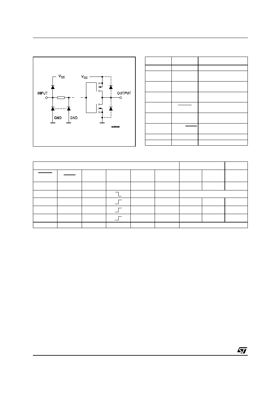
INPUT AND OUTPUT EQUIVALENT CIRCUIT
PIN DESCRIPTION
TRUTH TABLE
X : Don't Care
a........h : The level of steady input voltage at inputs a through H respectively
PIN No
SYMBOL
NAME AND FUNCTION
1
SI
Serial Data Inputs
2, 3, 4, 5, 10,
11, 12, 14
A to H
Parallel Data Inputs
6
CLOCK INH
Clock Enable Input
(Active Low)
7
CLOCK
Clock Input (LOW to
HIGH, Edge Triggered
9
CLEAR
Asynchronous Master
Reset Input (Active Low)
13
Q
H
Serial Output from the
Last Stage
15
SHIFT/LOAD
Parallel Enable Input
(Active Low)
8
GND
Ground (0V)
16
Vcc
Positive Supply Voltage
INPUTS
INTERNAL OUTPUTS
OUTPUTS
CLEAR
SHIFT/
LOAD
CLOCK
INH
CLOCK
SERIAL IN
PARALLEL
A..........H
QA
QB
QH
L
X
X
X
X
X
L
L
L
L
X
X
X
X
NO CHANGE
H
L
L
X
a..............h
a
b
h
H
H
L
H
X
H
QAn
QGn
H
H
L
L
X
L
QAn
QGn
H
X
H
X
X
X
NO CHANGE

M74HC166
4/12
ABSOLUTE MAXIMUM RATINGS
Absolute Maximum Ratings are those values beyond which damage to the device may occur. Functional operation under these conditions is
not implied
(*) 500mW at 65
∞
C; derate to 300mW by 10mW/
∞
C from 65
∞
C to 85
∞
C
RECOMMENDED OPERATING CONDITIONS
Symbol
Parameter
Value
Unit
V
CC
Supply Voltage
-0.5 to +7
V
V
I
DC Input Voltage
-0.5 to V
CC
+ 0.5
V
V
O
DC Output Voltage
-0.5 to V
CC
+ 0.5
V
I
IK
DC Input Diode Current
±
20
mA
I
OK
DC Output Diode Current
±
20
mA
I
O
DC Output Current
±
25
mA
I
CC
or I
GND
DC V
CC
or Ground Current
±
50
mA
P
D
Power Dissipation
500(*)
mW
T
stg
Storage Temperature
-65 to +150
∞C
T
L
Lead Temperature (10 sec)
300
∞C
Symbol
Parameter
Value
Unit
V
CC
Supply Voltage
2 to 6
V
V
I
Input Voltage
0 to V
CC
V
V
O
Output Voltage
0 to V
CC
V
T
op
Operating Temperature
-55 to 125
∞C
t
r
, t
f
Input Rise and Fall Time
V
CC
= 2.0V
0 to 1000
ns
V
CC
= 4.5V
0 to 500
ns
V
CC
= 6.0V
0 to 400
ns

