1/11
July 2001
s
HIGH SPEED :
f
MAX
= 66MHz (TYP.) at V
CC
= 6V
s
LOW POWER DISSIPATION:
I
CC
=4
µ
A(MAX.) at T
A
=25∞C
s
HIGH NOISE IMMUNITY:
V
NIH
= V
NIL
= 28 % V
CC
(MIN.)
s
SYMMETRICAL OUTPUT IMPEDANCE:
|I
OH
| = I
OL
= 4mA (MIN)
s
BALANCED PROPAGATION DELAYS:
t
PLH
t
PHL
s
WIDE OPERATING VOLTAGE RANGE:
V
CC
(OPR) = 2V to 6V
s
PIN AND FUNCTION COMPATIBLE WITH
74 SERIES 174
DESCRIPTION
The M74HC174 is an high speed CMOS HEX
D-TYPE FLIP FLOP WITH CLEAR fabricated with
silicon gate C
2
MOS technology.
Information signals applied to D inputs are
transferred to the Q output on the positive going
edge of the clock pulse. When the CLEAR input is
held low, the Q outputs are held low independently
of the other inputs.
All inputs are equipped with protection circuits
against static discharge and transient excess
voltage.
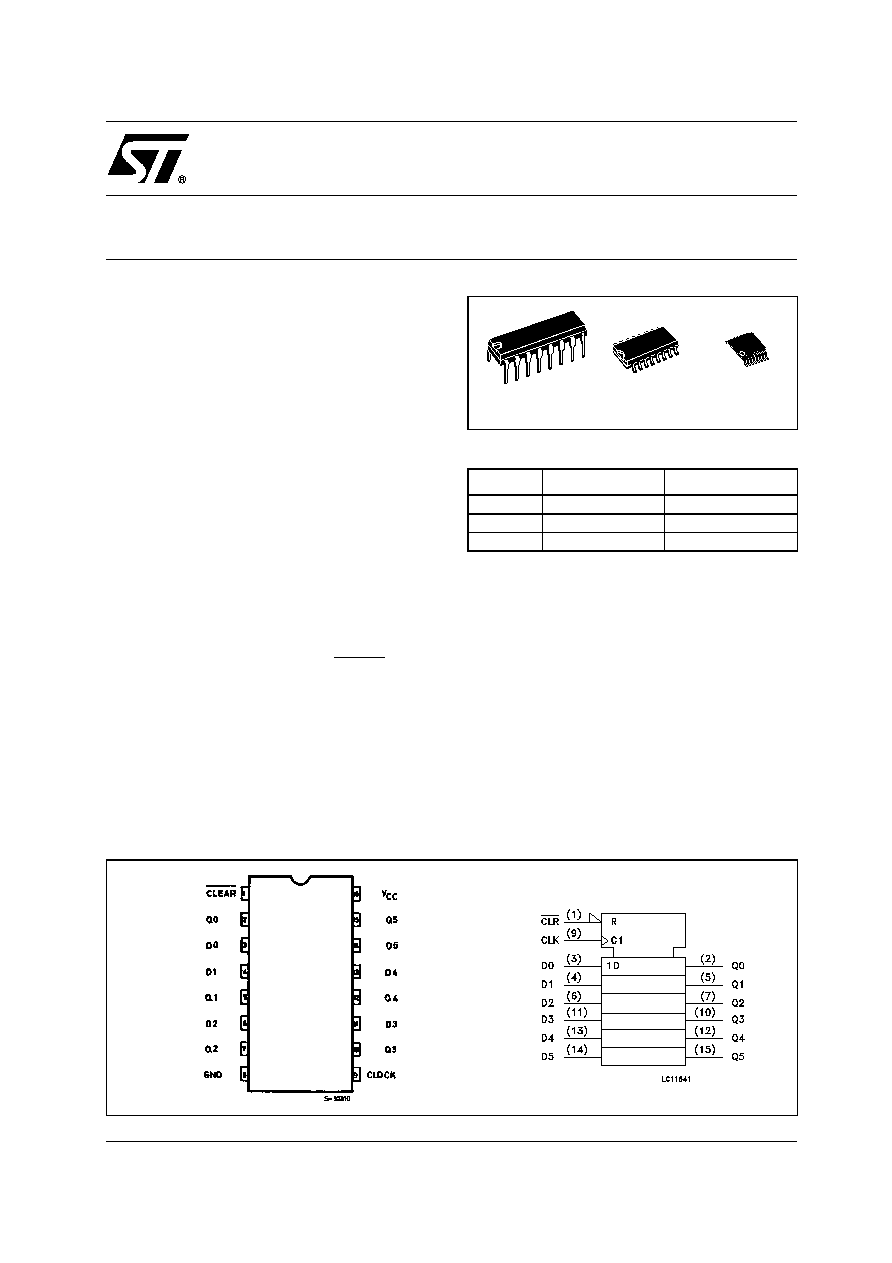
M74HC174
HEX D-TYPE FLIP FLOP WITH CLEAR
PIN CONNECTION AND IEC LOGIC SYMBOLS
ORDER CODES
PACKAGE
TUBE
T & R
DIP
M74HC174B1R
SOP
M74HC174M1R
M74HC174RM13TR
TSSOP
M74HC174TTR
TSSOP
DIP
SOP
M74HC174
2/11
INPUT AND OUTPUT EQUIVALENT CIRCUIT
PIN DESCRIPTION
TRUTH TABLE
X : Don't Care
LOGIC DIAGRAM
This logic diagram has not to be used to estimate propagation delays
PIN No
SYMBOL
NAME AND FUNCTION
1
CLEAR
Asynchronous Master
Reset (Active Low)
2, 5, 7, 10,
12, 15
Q0 to Q5
Flip-Flop Outputs
3, 4, 6, 11,
13, 14
D0 to D5
Data Inputs
9
CLOCK
Clock Input (LOW to
HIGH, edge triggered)
8
GND
Ground (0V)
16
Vcc
Positive Supply Voltage
INPUTS
OUTPUTS
FUNCTION
CLEAR
D
CK
Q
L
X
X
L
CLEAR
H
L
L
H
H
H
H
X
Qn
NO CHANGE
M74HC174
3/11
ABSOLUTE MAXIMUM RATINGS
Absolute Maximum Ratings are those values beyond which damage to the device may occur. Functional operation under these conditions is
not implied
(*) 500mW at 65
∞
C; derate to 300mW by 10mW/
∞
C from 65
∞
C to 85
∞
C
RECOMMENDED OPERATING CONDITIONS
Symbol
Parameter
Value
Unit
V
CC
Supply Voltage
-0.5 to +7
V
V
I
DC Input Voltage
-0.5 to V
CC
+ 0.5
V
V
O
DC Output Voltage
-0.5 to V
CC
+ 0.5
V
I
IK
DC Input Diode Current
±
20
mA
I
OK
DC Output Diode Current
±
20
mA
I
O
DC Output Current
±
25
mA
I
CC
or I
GND
DC V
CC
or Ground Current
±
50
mA
P
D
Power Dissipation
500(*)
mW
T
stg
Storage Temperature
-65 to +150
∞C
T
L
Lead Temperature (10 sec)
300
∞C
Symbol
Parameter
Value
Unit
V
CC
Supply Voltage
2 to 6
V
V
I
Input Voltage
0 to V
CC
V
V
O
Output Voltage
0 to V
CC
V
T
op
Operating Temperature
-55 to 125
∞C
t
r
, t
f
Input Rise and Fall Time
V
CC
= 2.0V
0 to 1000
ns
V
CC
= 4.5V
0 to 500
ns
V
CC
= 6.0V
0 to 400
ns
M74HC174
4/11
DC SPECIFICATIONS
Symbol
Parameter
Test Condition
Value
Unit
V
CC
(V)
T
A
= 25∞C
-40 to 85∞C
-55 to 125∞C
Min.
Typ.
Max.
Min.
Max.
Min.
Max.
V
IH
High Level Input
Voltage
2.0
1.5
1.5
1.5
V
4.5
3.15
3.15
3.15
6.0
4.2
4.2
4.2
V
IL
Low Level Input
Voltage
2.0
0.5
0.5
0.5
V
4.5
1.35
1.35
1.35
6.0
1.8
1.8
1.8
V
OH
High Level Output
Voltage
2.0
I
O
=-20
µ
A
1.9
2.0
1.9
1.9
V
4.5
I
O
=-20
µ
A
4.4
4.5
4.4
4.4
6.0
I
O
=-20
µ
A
5.9
6.0
5.9
5.9
4.5
I
O
=-4.0 mA
4.18
4.31
4.13
4.10
6.0
I
O
=-5.2 mA
5.68
5.8
5.63
5.60
V
OL
Low Level Output
Voltage
2.0
I
O
=20
µ
A
0.0
0.1
0.1
0.1
V
4.5
I
O
=20
µ
A
0.0
0.1
0.1
0.1
6.0
I
O
=20
µ
A
0.0
0.1
0.1
0.1
4.5
I
O
=4.0 mA
0.17
0.26
0.33
0.40
6.0
I
O
=5.2 mA
0.18
0.26
0.33
0.40
I
I
Input Leakage
Current
6.0
V
I
= V
CC
or GND
±
0.1
±
1
±
1
µ
A
I
CC
Quiescent Supply
Current
6.0
V
I
= V
CC
or GND
4
40
80
µ
A
M74HC174
5/11
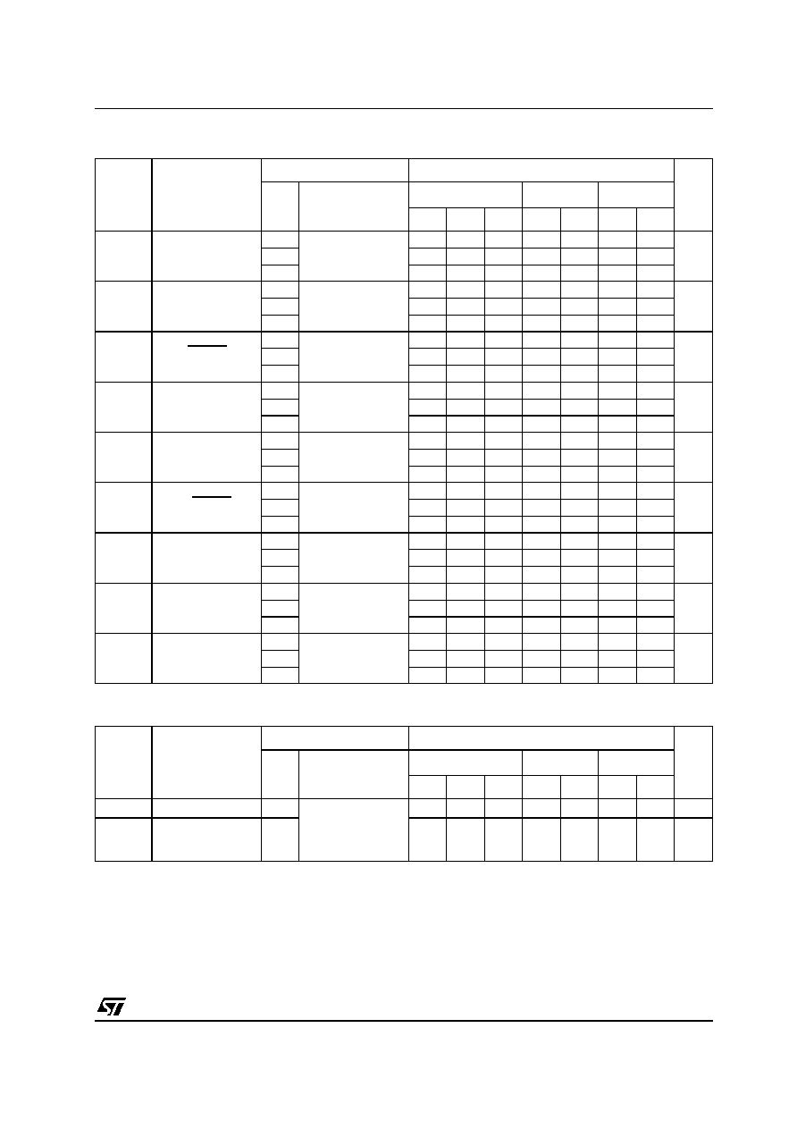
AC ELECTRICAL CHARACTERISTICS (C
L
= 50 pF, Input t
r
= t
f
= 6ns)
CAPACITIVE CHARACTERISTICS
1) C
PD
is defined as the value of the IC's internal equivalent capacitance which is calculated from the operating current consumption without
load. (Refer to Test Circuit). Average operating current can be obtained by the following equation. I
CC(opr)
= C
PD
x V
CC
x f
IN
+ I
CC
/6 (per FLIP/
FLOP)
And the total CPD when N pcs of FLIP-FLOP operate can be gained by the following equation : CPD (total) = 38 + 15 x n
Symbol
Parameter
Test Condition
Value
Unit
V
CC
(V)
T
A
= 25∞C
-40 to 85∞C
-55 to 125∞C
Min.
Typ.
Max.
Min.
Max.
Min.
Max.
t
TLH
t
THL
Output Transition
Time
2.0
30
75
95
110
ns
4.5
8
15
19
22
6.0
7
13
16
19
t
PLH
t
PHL
Propagation Delay
Time (CLOCK - Q)
2.0
68
135
170
205
ns
4.5
17
27
34
41
6.0
14
23
29
35
t
PLH
t
PHL
Propagation Delay
Time (CLEAR - Q)
2.0
72
145
180
220
ns
4.5
18
29
36
44
6.0
15
25
31
37
f
MAX
Maximum Clock
Frequency
2.0
7.2
14
5.8
4.8
MHz
4.5
36
56
29
24
6.0
42
66
34
28
t
W(H)
t
W(L)
Minimum Pulse
Width (CLOCK)
2.0
24
75
95
110
ns
4.5
6
15
19
22
6.0
5
13
16
19
t
W(L)
Minimum Pulse
Width (CLEAR)
2.0
24
75
95
110
ns
4.5
6
15
19
22
6.0
5
13
16
19
t
s
Minimum Set-up
Time
2.0
28
75
95
110
ns
4.5
7
15
19
22
6.0
6
13
16
19
t
h
Minimum Hold
Time
2.0
0
0
0
ns
4.5
0
0
0
6.0
0
0
0
t
REM
Minimum Removal
Time
2.0
5
5
5
5
ns
4.5
5
5
5
5
6.0
5
5
5
5
Symbol
Parameter
Test Condition
Value
Unit
V
CC
(V)
T
A
= 25∞C
-40 to 85∞C
-55 to 125∞C
Min.
Typ.
Max.
Min.
Max.
Min.
Max.
C
IN
Input Capacitance
5.0
5
10
10
10
pF
C
PD
Power Dissipation
Capacitance (note
1)
5.0
40
pF