
1/14
August 2001
s
HIGH SPEED :
f
MAX
= 61 MHz (TYP.) at V
CC
= 6V
s
LOW POWER DISSIPATION:
I
CC
=4
µ
A(MAX.) at T
A
=25∞C
s
HIGH NOISE IMMUNITY:
V
NIH
= V
NIL
= 28 % V
CC
(MIN.)
s
SYMMETRICAL OUTPUT IMPEDANCE:
|I
OH
| = I
OL
= 4mA (MIN)
s
BALANCED PROPAGATION DELAYS:
t
PLH
t
PHL
s
WIDE OPERATING VOLTAGE RANGE:
V
CC
(OPR) = 2V to 6V
s
PIN AND FUNCTION COMPATIBLE WITH
74 SERIES 191
DESCRIPTION
The M74HC191 is an high speed CMOS 4-BIT
SYNCHRONOUS UP/DOWN COUNTER
fabricated with silicon gate C
2
MOS technology.
State changes of the counter are synchronous
with the LOW-to-HIGH transition of the Clock
Pulse Input.
An asynchronous parallel load input overrides
counting and loads the data present on the DATA
inputs into the flip-flops, which makes it possible to
use the circuits as programmable counters. A
count enable input serves as the carry/borrow
input in multi-stage counters. Control input, Down/
Up, determines whether a circuit counts up or
down. A MAX/MIN output and a Ripple Clock
output provide overflow/underflow indication and
make possible a variety of methods for generating
carry/borrow signals in multi-stage counter
applications.
All inputs are equipped with protection circuits
against static discharge and transient excess
voltage.
M74HC191
4 BIT SYNCHRONOUS UP/DOWN COUNTERS
PIN CONNECTION AND IEC LOGIC SYMBOLS
ORDER CODES
PACKAGE
TUBE
T & R
DIP
M74HC191B1R
SOP
M74HC191M1R
M74HC191RM13TR
TSSOP
M74HC191TTR
TSSOP
DIP
SOP
M74HC191
2/14
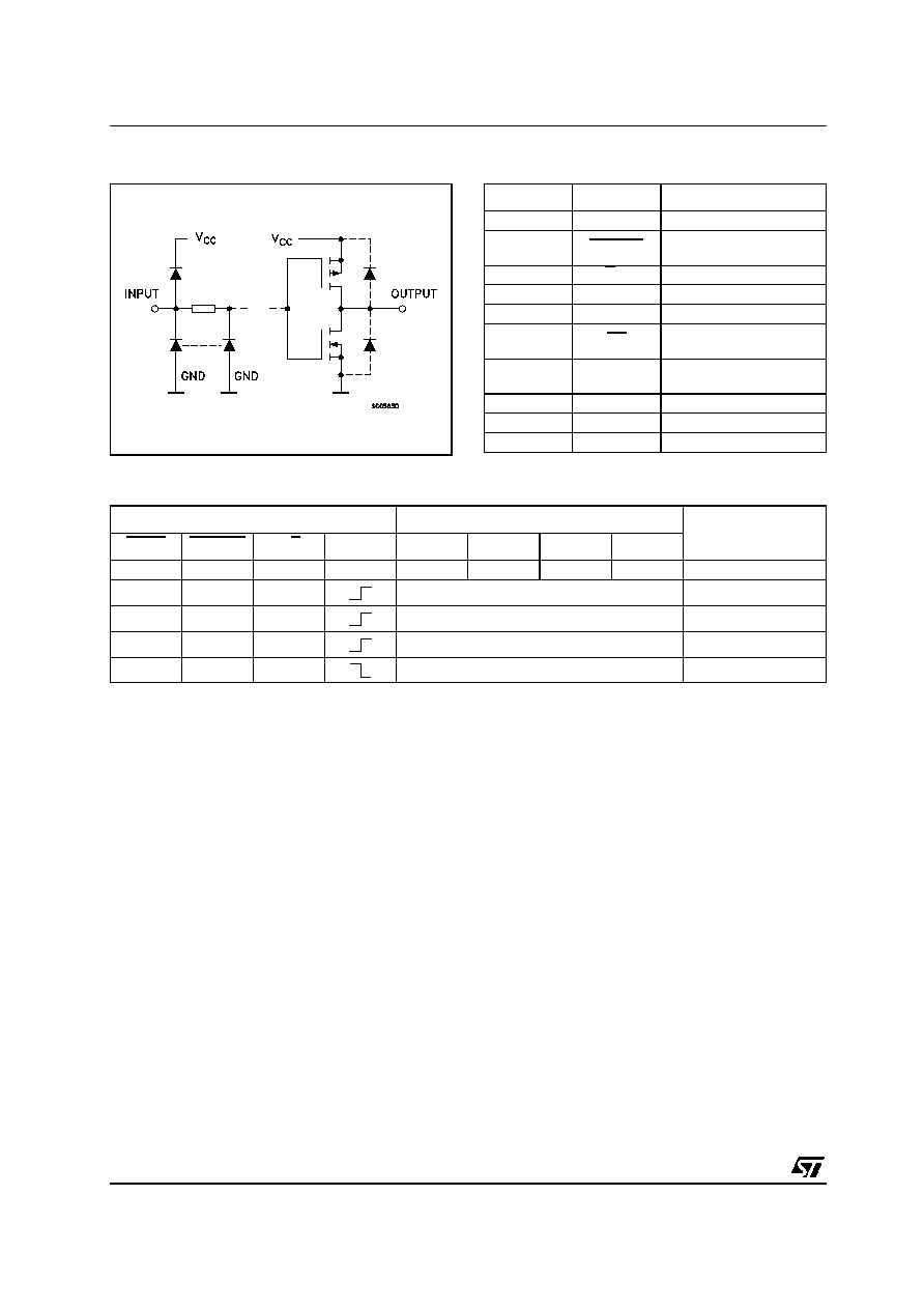
INPUT AND OUTPUT EQUIVALENT CIRCUIT
PIN DESCRIPTION
TRUTH TABLE
X : Don't Care
a - d : The level of steady state inputs a through d respectively
PIN No
SYMBOL
NAME AND FUNCTION
3, 2, 6, 7
QA to QD
Flip-Flop Outputs
4
ENABLE
Count Enable Input
(Active LOW)
5
U/D
Parallel Data Input
11
LOAD
Load Input (Active LOW)
12
MA/MI OUT Terminal Count Output
13
RC
Ripple Clock Output
(Active LOW)
14
CLOCK
Clock Input (LOW to
HIGH, edge triggered)
15, 1, 10, 9
DA to DD
Data Inputs
8
GND
Ground (0V)
16
Vcc
Positive Supply Voltage
INPUTS OUTPUTS
FUNCTION
LOAD
ENABLE
D/U
CLOCK
QA
QB
QC
QD
L
X
X
X
a
b
c
d
PRESET DATA
H
L
L
UP COUNT
UP COUNT
H
L
H
DOWN COUNT
DOWN COUNT
H
H
X
NO CHANGE
NO COUNT
H
X
X
NO CHANGE
NO COUNT

M74HC191
4/14
TIMING CHART
ABSOLUTE MAXIMUM RATINGS
Absolute Maximum Ratings are those values beyond which damage to the device may occur. Functional operation under these conditions is
not implied
(*) 500mW at 65
∞
C; derate to 300mW by 10mW/
∞
C from 65
∞
C to 85
∞
C
Symbol
Parameter
Value
Unit
V
CC
Supply Voltage
-0.5 to +7
V
V
I
DC Input Voltage
-0.5 to V
CC
+ 0.5
V
V
O
DC Output Voltage
-0.5 to V
CC
+ 0.5
V
I
IK
DC Input Diode Current
±
20
mA
I
OK
DC Output Diode Current
±
20
mA
I
O
DC Output Current
±
25
mA
I
CC
or I
GND
DC V
CC
or Ground Current
±
50
mA
P
D
Power Dissipation
500(*)
mW
T
stg
Storage Temperature
-65 to +150
∞C
T
L
Lead Temperature (10 sec)
300
∞C

