
M54HC221/221A
M74HC221/221A
October 1993
DUAL MONOSTABLE MULTIVIBRATOR
B1R
(Plastic Package)
ORDER CODES :
M54HCXXXF1R
M74HCXXXXM1R
M74HCXXXB1R
M74HCXXXC1R
F1R
(Ceramic Package)
M1R
(Micro Package)
C1R
(Chip Carrier)
PIN CONNECTIONS (top view)
NC =
No Internal
Connection
.
HIGH SPEED
t
PD
= 25 ns (TYP) at V
CC
= 5V
.
LOW POWER DISSIPATION
STANDBY STATE I
CC
=4
�
A (MAX.) AT T
A
=25
�
C
ACTIVE STATE I
CC
= 700
�
A (MAX.) AT V
CC
=5V
.
HIGH NOISE IMMUNITY
V
NIH
= V
NIL
= 28 % V
CC
(MIN.)
.
OUTPUT DRIVE CAPABILITY
10 LSTTL LOADS
.
SYMMETRICAL OUTPUT IMPEDANCE
I
OH
= I
OL
= 4 mA (MIN.)
.
BALANCED PROPAGATION DELAYS
t
PLH
= t
PHL
.
WIDE OPERATING VOLTAGE RANGE
V
CC
(OPR) = 2 V TO 6 V
.
WIDE OUTPUT PULSE WIDTH RANGE
t
WOUT
= 150 ns
60 s OVER AT V
CC
= 4.5 V
.
PIN AND FUNCTION COMPATIBLE WITH
54/74LS221
The M54/74HC221/221A are high speed CMOS
MONOSTABLE multivibrators fabricated with sili-
con gate C
2
MOS technology. It achieves the high
speed operation similar to equivalent LSTTL while
maintaining the CMOS low power dissipation. There
are two trigger inputs, A INPUT (negative edge) and
B INPUT (positive edge). Triggering on the B input
occurs at a particular voltage threshold and is not re-
lated to the rise and fall time of the applied pulse.
The device may also be triggered by using the CLR
input (positive-edge) because of the Schmitt-trigger
input ; after triggering the output maintains the
MONOSTABLEstate for the time period determined
by the external resistor Rx and capacitor Cx.Taking
CLR low breaks this MONOSTABLE STATE. If the
next trigger pulse occurs during the MONOSTABLE
period it makes the MONOSTABLE period longer.
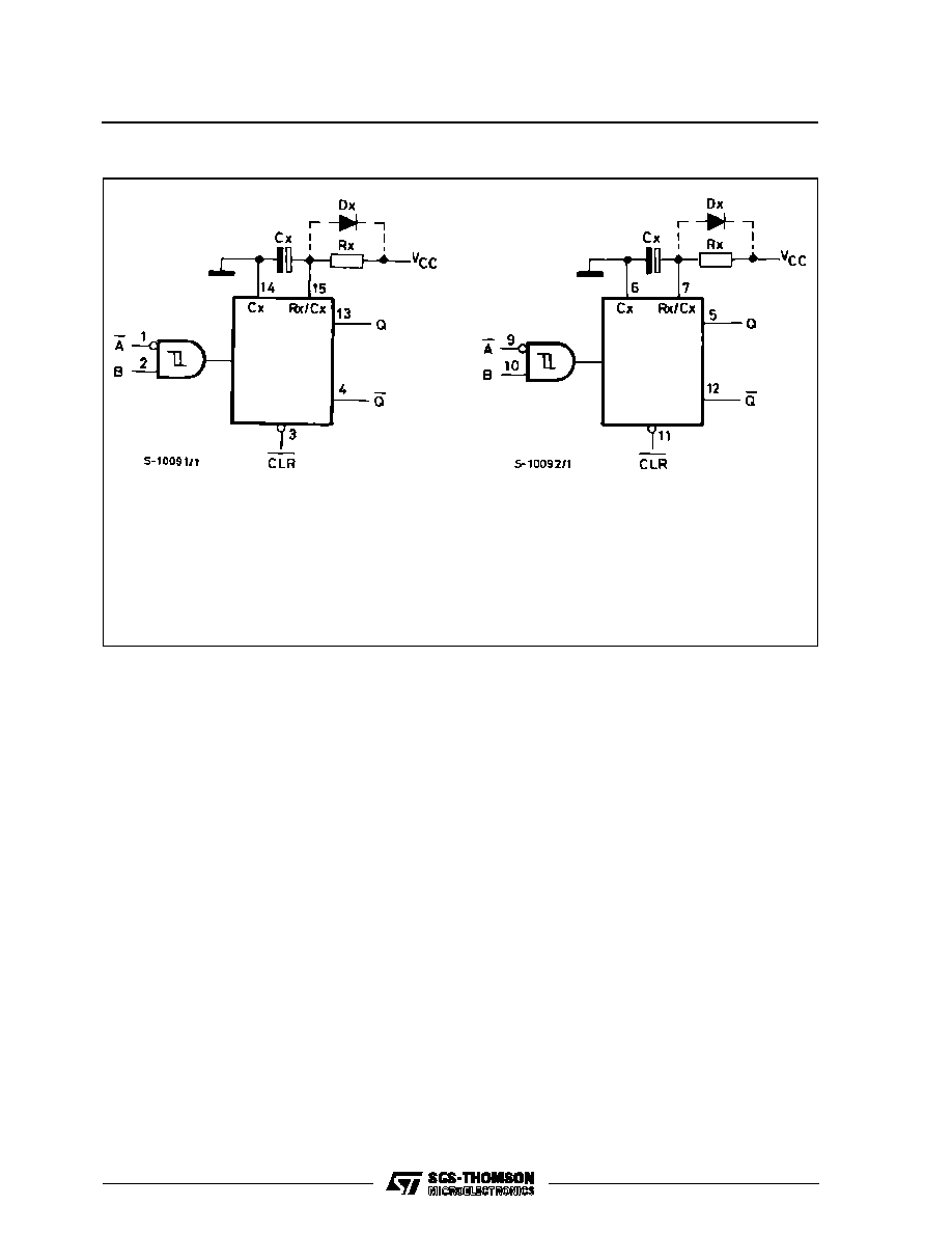
Limit for values of Cx and Rx :
Cx : NO LIMIT
Rx : V
CC
< 3.0 V 5 K
to 1 M
V
CC
3.0 V 1 K
to 1 M
Two different pulse width constants are available:
K
0.7 for HC221
K
1 for HC221A
All inputs are equipped with protection circuits
against static discharge and transient excess volt-
age.
DESCRIPTION
1/14
BLOCK DIAGRAM
Note :
(1) Cx, Rx, Dx are external components.
(2) Dx is a clamping diode.
The external capacitor is charged to V
CC
inthe stand-by state, i.e. no trigger. When the supply voltage is turned off Cx is discharged mainly
through an internal parasitic diode (see figures). If Cx is sufficiently large and V
CC
decreases rapidy, there will be some possibility of da-
maging the I.C. with a surge current or latch-up. If the voltage supply filter capacitor is large enough and V
CC
decrease slowly, the surge
current is automatically limited and damage the I.C. is avoided. The maximum forward current of the parasitic diode is approximately 20
mA. In cases where Cx is large the time taken for the supply voltage to fall to 0.4 V
CC
can be calculated as follows :
t
f
(V
CC
� 0.7)
Cx/20mA
In cases where t
f
is too short an external clamping diode is required to protect the I.C. from the surge current.
FUNCTIONAL DESCRIPTION
STAND-BY STATE
The external capacitor, Cx, is fully charged to V
CC
in the stand-by state. Hence, before triggering, tran-
sistor Qp and Qn (connected to the Rx/Cx node) are
both turned-off. The two comparators that control
the timing and the two reference voltage sources
stop operating. The total supply current is therefore
only leakage current.
TRIGGER OPERATION
Triggering occurs when :
1
st
) A is "low" and B has a falling edge ;
2
nd
) B is "high" and A has a rising edge ;
3
rd
) A is low and B is high and C1 has a rising edge.
After the multivibrator has been retriggered com-
parator C1 and C2 start operating and Qn is turned
on. Cx then discharges through Qn. The voltage at
the node R/C external falls.
When it reaches V
REFL
the output of comparator C1
becomes low. This in turn resets the flip-flop and Qn
is turned off.
At this point C1 stops functioning but C2 continues
to operate.
The voltage at R/C external begins to rise with a time
constant set by the external components Rx, Cx.
Triggering the multivibrator causes Q to go high after
internal delay due to the flip-flop and the gate. Q re-
mains high until the voltage at R/C external rises
again to V
REFH
. At this point C2 output goes low and
O goes low. C2 stop operating. That means that
after triggering when the voltage R/C external re-
turns to V
REFH
the multivibrator has returned to its
MONOSTABLE STATE. In the case where Rx
Cx
are large enough and the discharge time of the ca-
pacitor and the delay time in the I.C. can be ignored,
the width of the output pulse tw (out) is as follows :
t
W(OUT)
= 0.70 Cx
Rx (HC221)
t
W(OUT)
= Cx
Rx (HC221A)
RESET OPERATION
CL is normally high. If CL is low, the trigger is not ef-
fective because Q output goes low and trigger con-
trol flip-flop is reset.
Also transistor Op is turned on and Cx is charged
quicky to V
CC
. This means if CL input goes low, the
IC becomes waiting state both in operating and non
operating state.
M54/M74HC221/221A
3/14

TRUTH TABLE
INPUTS
OUTPUTS
NOTE
A
B
CLR
Q
Q
H
H
OUTPUT ENABLE
X
L
H
L (*)
H (*)
INHIBIT
H
X
H
L (*)
H (*)
INHIBIT
L
H
OUTPUT ENABLE
L
H
OUTPUT ENABLE
X
X
L
L
H
INHIBIT
X: Don't Care
(*): Except for monostble period
INPUT AND OUTPUT EQUIVALENT CIRCUIT
PIN DESCRIPTION
PIN No
SYMBOL
NAME AND FUNCTION
1, 9
1A, 2A
Trigger Inputs (Negative
Edge Triggered)
2, 10
1B, 2B
Trigger Inputs (Positive
Edge Triggered)
3, 11
1CLR,
2CLR
Direct Reset LOW and
Trigger Action at Positive
Edge
4, 12
1Q, 2Q
Outputs (Active LOW)
7
2R
EXT
/C
EXT
External Resistor
Capacitor Connection
13, 5
1Q, 2Q
Outputs (Active HIGH)
14, 6
1C
EXT
2C
EXT
External Capacitor
Connection
15
1R
EXT
/C
EXT
External Resistor
Capacitor Connection
8
GND
Ground (0V)
16
V
CC
Positive Supply Voltage
IEC LOGIC SYMBOL
M54/M74HC221/221A
4/14

ABSOLUTE MAXIMUM RATING
Symbol
Parameter
Value
Unit
V
CC
Supply Voltage
-0.5 to +7
V
V
I
DC Input Voltage
-0.5 to V
CC
+ 0.5
V
V
O
DC Output Voltage
-0.5 to V
CC
+ 0.5
V
I
IK
DC Input Diode Current
�
20
mA
I
OK
DC Output Diode Current
�
20
mA
I
O
DC Output Source Sink Current Per Output Pin
�
25
mA
I
CC
or I
GND
DC V
CC
or Ground Current
�
50
mA
P
D
Power Dissipation
500 (*)
mW
T
stg
Storage Temperature
-65 to +150
o
C
T
L
Lead Temperature (10 sec)
300
o
C
Absolute Maximum Ratings are those values beyond which damage to the device may occur. Functional operation under these condition is not implied.
(*) 500 mW:
65
o
C derate to 300 mW by 10mW/
o
C: 65
o
C to 85
o
C
RECOMMENDED OPERATING CONDITIONS
Symbol
Parameter
Value
Unit
V
CC
Supply Voltage
2 to 6
V
V
I
Input Voltage
0 to V
CC
V
V
O
Output Voltage
0 to V
CC
V
T
op
Operating Temperature: M54HC Series
M74HC Series
-55 to +125
-40 to +85
o
C
o
C
t
r
, t
f
Input Rise and Fall Time (CLR and A only)
V
CC
= 2 V
0 to 1000
ns
V
CC
= 4.5 V
0 to 500
V
CC
= 6 V
0 to 400
C
X
External Capacitor
> 100 (*)
pF
R
X
External Resistor
V
CC
< 3 V
5K to 1M (*)
V
CC
3 V
1K to 1M (*)
(*)The maximum allowable values of Cx and Rx are a function of leackage of capacitor Cx, the leackage of HC221/A, and leackage due to the
board layout and surface resistance. Susceptibility to externally induced noise signals may occur for Rx > 1M
M54/M74HC221/221A
5/14
