
1/11
July 2001
s
HIGH SPEED:
t
PD
= 16ns (TYP.) at V
CC
= 6V
s
LOW POWER DISSIPATION:
I
CC
= 4
µ
A(MAX.) at T
A
=25∞C
s
HIGH NOISE IMMUNITY:
V
NIH
= V
NIL
= 28 % V
CC
(MIN.)
s
SYMMETRICAL OUTPUT IMPEDANCE:
|I
OH
| = I
OL
= 4mA (MIN)
s
BALANCED PROPAGATION DELAYS:
t
PLH
t
PHL
s
WIDE OPERATING VOLTAGE RANGE:
V
CC
(OPR) = 2V to 6V
s
PIN AND FUNCTION COMPATIBLE WITH
74 SERIES 237
DESCRIPTION
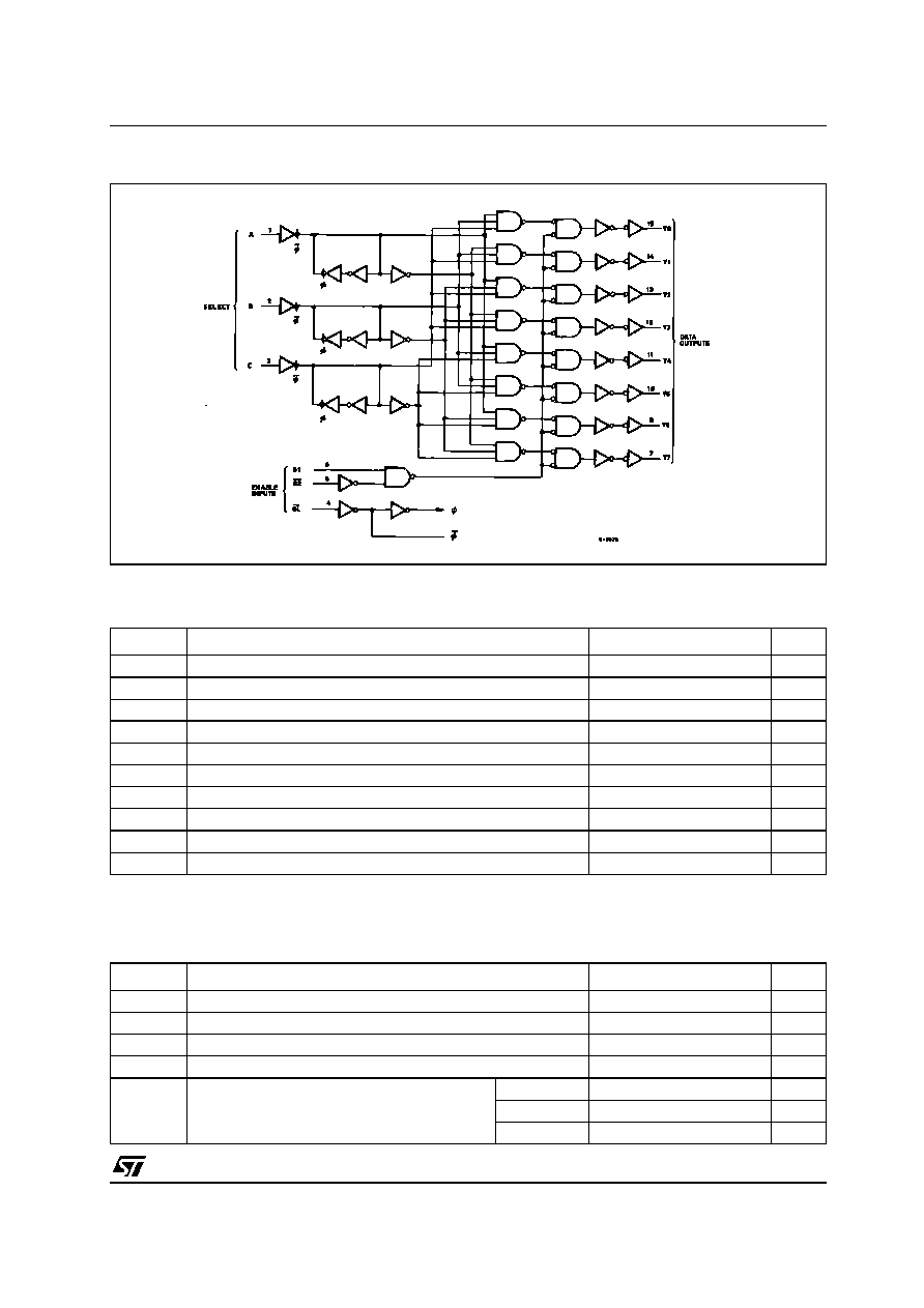
The M74HC237 is an high speed CMOS 3 TO 8
LINE DECODER fabricated with silicon gate
C
2
MOS technology.
When GL goes from low to high, the address
present at the select inputs (A, B, C) is stored in
the latches. As long as GL remains high no
address changes will be recognized. Output
enable controls, G1 and G2 control the state of the
outputs independently of the select or
latch-enable inputs. All of the outputs are low
unless G1 is high and G2 is low. The M74HC237
is ideally suited for the implementation of
glitch-free decoders in stored-address
applications in bus oriented systems.
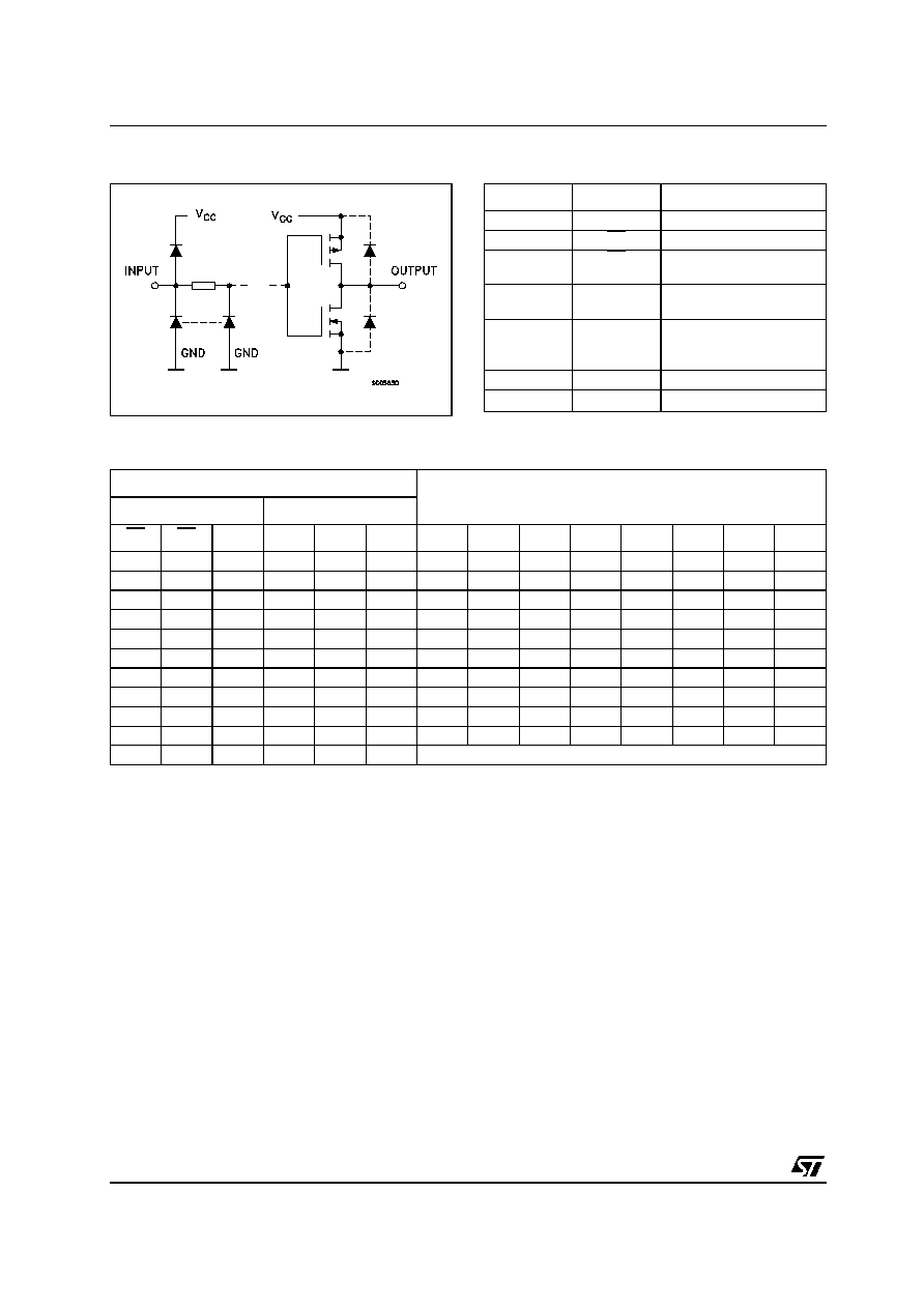
All inputs are equipped with protection circuits
against static discharge and transient excess
voltage.
M74HC237
3 TO 8 LINE DECODER LATCH
PIN CONNECTION AND IEC LOGIC SYMBOLS
ORDER CODES
PACKAGE
TUBE
T & R
DIP
M74HC237B1R
SOP
M74HC237M1R
M74HC237RM13TR
TSSOP
M74HC237TTR
TSSOP
DIP
SOP
M74HC237
2/11
INPUT AND OUTPUT EQUIVALENT CIRCUIT
PIN DESCRIPTION
TRUTH TABLE
X : Don't Care
PIN No
SYMBOL
NAME AND FUNCTION
1, 2, 3
A, B, C
Data Inputs
4
GL
Latch Enable Input
5
G2
Data Enable Input (Active
LOW)
6
G1
Data Enable Input (Active
HIGH)
15, 14, 13,
12, 11, 10, 9,
7
Y0 to Y7
Decoder Outputs
8
GND
Ground (0V)
16
V
CC
Positive Supply Voltage
INPUTS
OUTPUTS
ENABLE
SELECT
GL
G2
G1
C
B
A
Y0
Y1
Y2
Y3
Y4
Y5
Y6
Y7
X
X
L
X
X
X
L
L
L
L
L
L
L
L
X
H
X
X
X
X
L
L
L
L
L
L
L
L
L
L
H
L
L
L
H
L
L
L
L
L
L
L
L
L
H
L
L
H
L
H
L
L
L
L
L
L
L
L
H
L
H
L
L
L
H
L
L
L
L
L
L
L
H
L
H
H
L
L
L
H
L
L
L
L
L
L
H
H
L
L
L
L
L
L
H
L
L
L
L
L
H
H
L
H
L
L
L
L
L
H
L
L
L
L
H
H
H
L
L
L
L
L
L
L
H
L
L
L
H
H
H
H
L
L
L
L
L
L
L
H
H
L
H
X
X
X
Outputs corresponding to stored address H: all others L
M74HC237
3/11
LOGIC DIAGRAM
This logic diagram has not be used to estimate propagation delays
ABSOLUTE MAXIMUM RATINGS
Absolute Maximum Ratings are those values beyond which damage to the device may occur. Functional operation under these conditions is
not implied
(*) 500mW at 65
∞
C; derate to 300mW by 10mW/
∞
C from 65
∞
C to 85
∞
C
RECOMMENDED OPERATING CONDITIONS
Symbol
Parameter
Value
Unit
V
CC
Supply Voltage
-0.5 to +7
V
V
I
DC Input Voltage
-0.5 to V
CC
+ 0.5
V
V
O
DC Output Voltage
-0.5 to V
CC
+ 0.5
V
I
IK
DC Input Diode Current
±
20
mA
I
OK
DC Output Diode Current
±
20
mA
I
O
DC Output Current
±
25
mA
I
CC
or I
GND
DC V
CC
or Ground Current
±
50
mA
P
D
Power Dissipation
500(*)
mW
T
stg
Storage Temperature
-65 to +150
∞C
T
L
Lead Temperature (10 sec)
300
∞C
Symbol
Parameter
Value
Unit
V
CC
Supply Voltage
2 to 6
V
V
I
Input Voltage
0 to V
CC
V
V
O
Output Voltage
0 to V
CC
V
T
op
Operating Temperature
-55 to 125
∞C
t
r
, t
f
Input Rise and Fall Time
V
CC
= 2.0V
0 to 1000
ns
V
CC
= 4.5V
0 to 500
ns
V
CC
= 6.0V
0 to 400
ns

M74HC237
4/11
DC SPECIFICATIONS
Symbol
Parameter
Test Condition
Value
Unit
V
CC
(V)
T
A
= 25∞C
-40 to 85∞C
-55 to 125∞C
Min.
Typ.
Max.
Min.
Max.
Min.
Max.
V
IH
High Level Input
Voltage
2.0
1.5
1.5
1.5
V
4.5
3.15
3.15
3.15
6.0
4.2
4.2
4.2
V
IL
Low Level Input
Voltage
2.0
0.5
0.5
0.5
V
4.5
1.35
1.35
1.35
6.0
1.8
1.8
1.8
V
OH
High Level Output
Voltage
2.0
I
O
=-20
µ
A
1.9
2.0
1.9
1.9
V
4.5
I
O
=-20
µ
A
4.4
4.5
4.4
4.4
6.0
I
O
=-20
µ
A
5.9
6.0
5.9
5.9
4.5
I
O
=-4.0 mA
4.18
4.31
4.13
4.10
6.0
I
O
=-5.2 mA
5.68
5.8
5.63
5.60
V
OL
Low Level Output
Voltage
2.0
I
O
=20
µ
A
0.0
0.1
0.1
0.1
V
4.5
I
O
=20
µ
A
0.0
0.1
0.1
0.1
6.0
I
O
=20
µ
A
0.0
0.1
0.1
0.1
4.5
I
O
=4.0 mA
0.17
0.26
0.33
0.40
6.0
I
O
=5.2 mA
0.18
0.26
0.33
0.40
I
I
Input Leakage
Current
6.0
V
I
= V
CC
or GND
±
0.1
±
1
±
1
µ
A
I
CC
Quiescent Supply
Current
6.0
V
I
= V
CC
or GND
4
40
80
µ
A

M74HC237
5/11
AC ELECTRICAL CHARACTERISTICS (C
L
= 50 pF, Input t
r
= t
f
= 6ns)
CAPACITIVE CHARACTERISTICS
1) C
PD
is defined as the value of the IC's internal equivalent capacitance which is calculated from the operating current consumption without
load.
Symbol
Parameter
Test Condition
Value
Unit
V
CC
(V)
T
A
= 25∞C
-40 to 85∞C
-55 to 125∞C
Min.
Typ.
Max.
Min.
Max.
Min.
Max.
t
TLH
t
THL
Output Transition
Time
2.0
30
75
95
110
ns
4.5
8
15
19
22
6.0
7
13
16
19
t
PLH
t
PHL
Propagation Delay
Time (A, B, C - Y)
2.0
60
180
225
270
ns
4.5
19
36
45
54
6.0
16
31
38
46
t
PLH
t
PHL
Propagation Delay
Time (G1 - Y)
2.0
45
140
175
210
ns
4.5
15
28
35
42
6.0
13
24
30
36
t
PLH
t
PHL
Propagation Delay
Time (G2 - Y)
2.0
45
140
175
210
ns
4.5
15
28
35
42
6.0
13
24
30
36
t
PLH
t
PHL
Propagation Delay
Time (GL - Y)
2.0
65
190
240
285
ns
4.5
21
38
48
57
6.0
18
32
41
48
t
W(L)
Minimum Pulse
Width (GL)
2.0
10
75
95
110
ns
4.5
6
15
19
22
6.0
6
13
16
19
t
s
Minimum Set-up
Time (A, B, C - GL)
2.0
12
50
65
75
ns
4.5
3
10
13
15
6.0
2
9
11
13
t
h
Minimum Hold
Time (A, B, C - GL)
2.0
25
30
40
ns
4.5
5
6
8
6.0
5
5
7
Symbol
Parameter
Test Condition
Value
Unit
V
CC
(V)
T
A
= 25∞C
-40 to 85∞C
-55 to 125∞C
Min.
Typ.
Max.
Min.
Max.
Min.
Max.
C
IN
Input Capacitance
5.0
5
10
10
10
pF
C
PD
Power Dissipation
Capacitance (note
1)
5.0
52
pF