1/13
July 2001
s
HIGH SPEED :
t
PD
= 20 ns (TYP.) at V
CC
= 6V
s
LOW POWER DISSIPATION:
I
CC
=4
µ
A(MAX.) at T
A
=25∞C
s
HIGH NOISE IMMUNITY:
V
NIH
= V
NIL
= 28 % V
CC
(MIN.)
s
SYMMETRICAL OUTPUT IMPEDANCE:
|I
OH
| = I
OL
= 4mA (MIN)
s
BALANCED PROPAGATION DELAYS:
t
PLH
t
PHL
s
WIDE OPERATING VOLTAGE RANGE:
V
CC
(OPR) = 2V to 6V
s
PIN AND FUNCTION COMPATIBLE WITH
74 SERIES 259
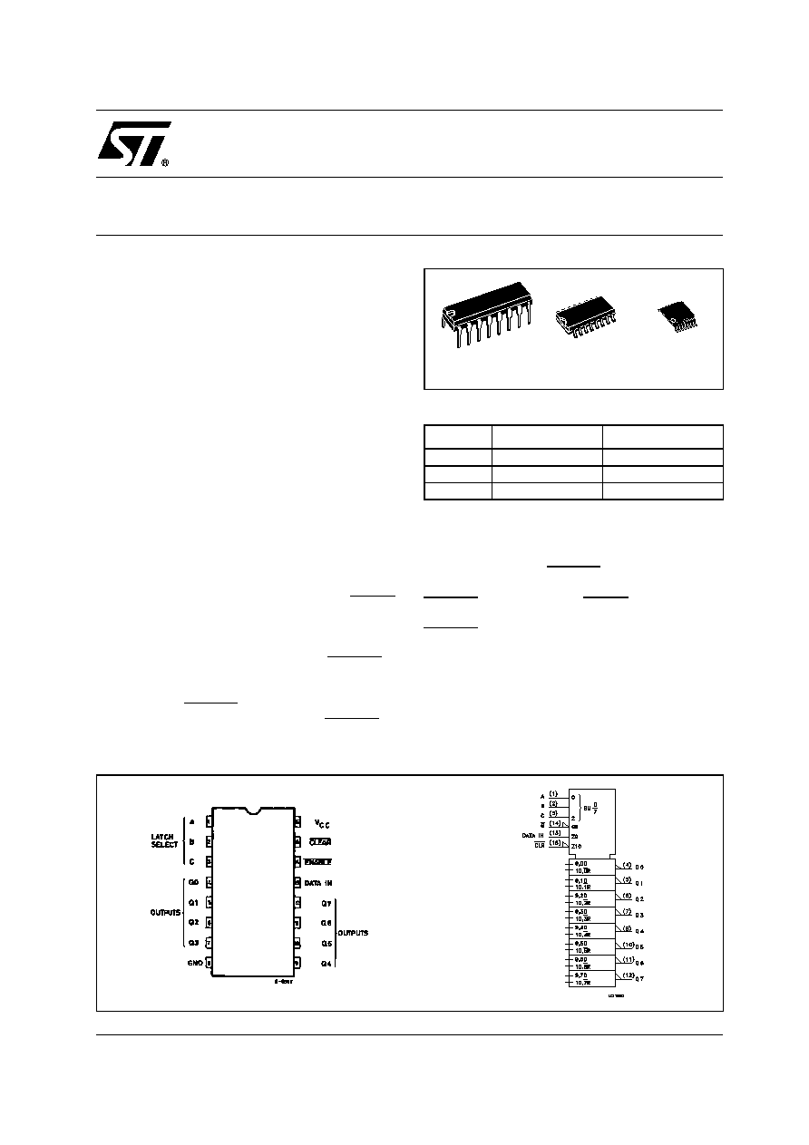
DESCRIPTION
The M74HC259 is an high speed CMOS 8 BIT
ADDRESSABLE LATCH fabricated with silicon
gate C
2
MOS technology.
The M74HC259 has single data input (D) 8 latch
outputs (Q0-Q7), 3 address inputs (A, B, and C),
common enable input (E), and a common CLEAR
input. To operate this device as an addressable
latch, data is held on the D input, and the address
of the latch into which the data is to be entered is
held on the A, B, and C inputs. When ENABLE is
taken low the data flows through to the addresses
output. The data is stored on the positive-going
edge of the ENABLE pulse. All unaddressed
latches will remain unaffected. With ENABLE in
the high state the device is deselected and all
latches remain in their previous state, unaffected
by changes on the data or address inputs. To
eliminate the possibility of entering erroneous data
into the latches, the ENABLE should be held high
(inactive) while the address lines are changing. If
ENABLE is held high and CLEAR is taken low all
eight latches are cleared to the low state. If
ENABLE is low all latches except the addressed
latch will be cleared. The addressed latch will
instead follow the D input, effectively
implementing a 3-to-8 line decoder.
All inputs are equipped with protection circuits
against static discharge and transient excess
voltage.
M74HC259
8 BIT ADDRESSABLE LATCH
PIN CONNECTION AND IEC LOGIC SYMBOLS
ORDER CODES
PACKAGE
TUBE
T & R
DIP
M74HC259B1R
SOP
M74HC259M1R
M74HC259RM13TR
TSSOP
M74HC259TTR
TSSOP
DIP
SOP
M74HC259
2/13
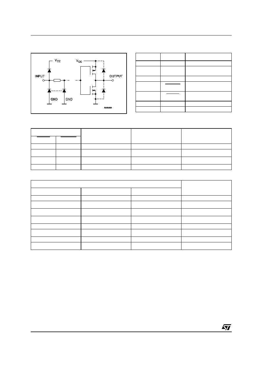
INPUT AND OUTPUT EQUIVALENT CIRCUIT
PIN DESCRIPTION
TRUTH TABLE
D : The level at the data input
Qi0 : The level before the indicated steady state input conditions where established, (i = 0, 1, ......., 7).
PIN No
SYMBOL
NAME AND FUNCTION
1, 2, 3
A, B, C
Address Inputs
4, 5, 6, 7, 9,
10, 11, 12
Q0 to Q7
Latch Outputs
13
D
Data Input
14
ENABLE
Latch Enable Input (Active
Low)
15
CLEAR
Conditional Reset Input
(Low)
8
GND
Ground (0V)
16
Vcc
Positive Supply Voltage
INPUTS
OUTPUTS OF
ADDRESSED LATCH
EACH OTHER OUTPUT
FUNCTION
CLEAR
ENABLE
H
L
D
Qi0
ADDRESSABLE LATCH
H
H
Qi0
Qi0
MEMORY
L
L
D
L
8 LINE DEMULTIPLEXER
L
H
L
L
CLEAR ALL BITS TO 'L'
SELECT INPUTS
LATCH ADDRESSED
C
B
A
L
L
L
Q0
L
L
H
Q1
L
H
L
Q2
L
H
H
Q3
H
L
L
Q4
H
L
H
Q5
H
H
L
Q6
H
H
H
Q7
M74HC259
3/13
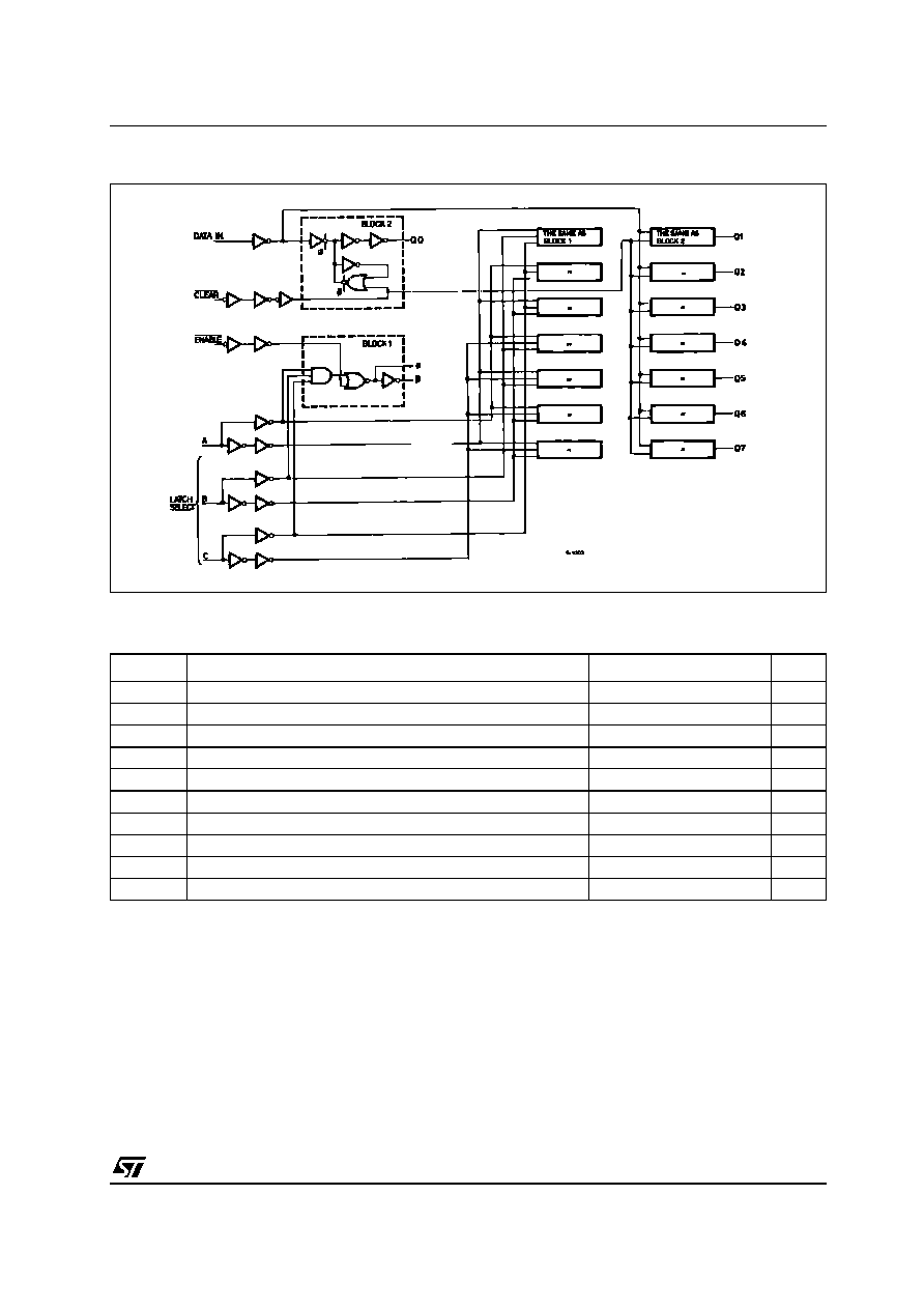
LOGIC DIAGRAM
This logic diagram has not be used to estimate propagation delays
ABSOLUTE MAXIMUM RATINGS
Absolute Maximum Ratings are those values beyond which damage to the device may occur. Functional operation under these conditions is
not implied
(*) 500mW at 65
∞
C; derate to 300mW by 10mW/
∞
C from 65
∞
C to 85
∞
C
Symbol
Parameter
Value
Unit
V
CC
Supply Voltage
-0.5 to +7
V
V
I
DC Input Voltage
-0.5 to V
CC
+ 0.5
V
V
O
DC Output Voltage
-0.5 to V
CC
+ 0.5
V
I
IK
DC Input Diode Current
±
20
mA
I
OK
DC Output Diode Current
±
20
mA
I
O
DC Output Current
±
25
mA
I
CC
or I
GND
DC V
CC
or Ground Current
±
50
mA
P
D
Power Dissipation
500(*)
mW
T
stg
Storage Temperature
-65 to +150
∞C
T
L
Lead Temperature (10 sec)
300
∞C
M74HC259
4/13
RECOMMENDED OPERATING CONDITIONS
DC SPECIFICATIONS
Symbol
Parameter
Value
Unit
V
CC
Supply Voltage
2 to 6
V
V
I
Input Voltage
0 to V
CC
V
V
O
Output Voltage
0 to V
CC
V
T
op
Operating Temperature
-55 to 125
∞C
t
r
, t
f
Input Rise and Fall Time
V
CC
= 2.0V
0 to 1000
ns
V
CC
= 4.5V
0 to 500
ns
V
CC
= 6.0V
0 to 400
ns
Symbol
Parameter
Test Condition
Value
Unit
V
CC
(V)
T
A
= 25∞C
-40 to 85∞C
-55 to 125∞C
Min.
Typ.
Max.
Min.
Max.
Min.
Max.
V
IH
High Level Input
Voltage
2.0
1.5
1.5
1.5
V
4.5
3.15
3.15
3.15
6.0
4.2
4.2
4.2
V
IL
Low Level Input
Voltage
2.0
0.5
0.5
0.5
V
4.5
1.35
1.35
1.35
6.0
1.8
1.8
1.8
V
OH
High Level Output
Voltage
2.0
I
O
=-20
µ
A
1.9
2.0
1.9
1.9
V
4.5
I
O
=-20
µ
A
4.4
4.5
4.4
4.4
6.0
I
O
=-20
µ
A
5.9
6.0
5.9
5.9
4.5
I
O
=-4.0 mA
4.18
4.31
4.13
4.10
6.0
I
O
=-5.2 mA
5.68
5.8
5.63
5.60
V
OL
Low Level Output
Voltage
2.0
I
O
=20
µ
A
0.0
0.1
0.1
0.1
V
4.5
I
O
=20
µ
A
0.0
0.1
0.1
0.1
6.0
I
O
=20
µ
A
0.0
0.1
0.1
0.1
4.5
I
O
=4.0 mA
0.17
0.26
0.33
0.40
6.0
I
O
=5.2 mA
0.18
0.26
0.33
0.40
I
I
Input Leakage
Current
6.0
V
I
= V
CC
or GND
±
0.1
±
1
±
1
µ
A
I
CC
Quiescent Supply
Current
6.0
V
I
= V
CC
or GND
4
40
80
µ
A
M74HC259
5/13
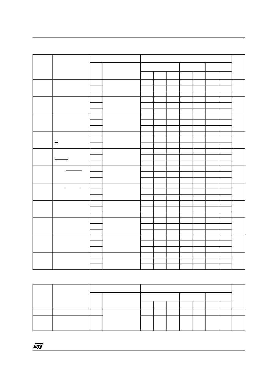
AC ELECTRICAL CHARACTERISTICS (C
L
= 50 pF, Input t
r
= t
f
= 6ns)
CAPACITIVE CHARACTERISTICS
1) C
PD
is defined as the value of the IC's internal equivalent capacitance which is calculated from the operating current consumption without
load. (Refer to Test Circuit). Average operating current can be obtained by the following equation. I
CC(opr)
= C
PD
x V
CC
x f
IN
+ I
CC
Symbol
Parameter
Test Condition
Value
Unit
V
CC
(V)
T
A
= 25∞C
-40 to 85∞C
-55 to 125∞C
Min.
Typ.
Max.
Min.
Max.
Min.
Max.
t
TLH
t
THL
Output Transition
Time
2.0
30
75
95
110
ns
4.5
8
15
19
22
6.0
7
13
16
19
t
PLH
t
PHL
Propagation Delay
Time
(DATA - Q)
2.0
56
140
175
210
ns
4.5
18
28
35
42
6.0
15
24
30
36
t
PLH
t
PHL
Propagation Delay
Time
(A, B, C - Q)
2.0
76
190
240
285
ns
4.5
24
38
48
57
6.0
20
32
41
48
t
PLH
t
PHL
Propagation Delay
Time
(G - Q)
2.0
57
150
190
225
ns
4.5
19
30
38
45
6.0
16
26
32
38
t
PLH
t
PHL
Propagation Delay
Time
(CLEAR - Q)
2.0
45
115
145
175
ns
4.5
15
23
29
35
6.0
13
20
25
30
t
W(L)
Minimum Pulse
Width (ENABLE)
2.0
28
75
90
115
ns
4.5
7
15
19
23
6.0
6
13
16
20
t
W(L)
Minimum Pulse
Width (CLEAR)
2.0
24
75
90
115
ns
4.5
6
15
19
23
6.0
5
13
16
20
t
s
Minimum Set-up
Time (DATA)
2.0
12
50
60
75
ns
4.5
3
10
12
15
6.0
3
9
11
13
t
s
Minimum Set-up
Time (A, B, C)
2.0
25
30
40
ns
4.5
5
6
8
6.0
5
5
7
t
h
Minimum Hold
Time (DATA)
2.0
5
5
5
ns
4.5
5
5
5
6.0
5
5
5
t
h
Minimum Hold
Time (A, B, C)
2.0
0
0
0
ns
4.5
0
0
0
6.0
0
0
0
Symbol
Parameter
Test Condition
Value
Unit
V
CC
(V)
T
A
= 25∞C
-40 to 85∞C
-55 to 125∞C
Min.
Typ.
Max.
Min.
Max.
Min.
Max.
C
IN
Input Capacitance
5.0
5
10
10
10
pF
C
PD
Power Dissipation
Capacitance (note
1)
5.0
66
pF