1/11
May 2004
s
HIGH SPEED:
t
PD
= 10ns (TYP.) at V
CC
= 6V
s
LOW POWER DISSIPATION:
I
CC
= 4
µ
A(MAX.) at T
A
=25∞C
s
HIGH NOISE IMMUNITY:
V
NIH
= V
NIL
= 28% V
CC
(MIN.)
s
SYMMETRICAL OUTPUT IMPEDANCE:
|I
OH
| = I
OL
= 6mA (MIN)
s
BALANCED PROPAGATION DELAYS:
t
PLH
t
PHL
s
WIDE OPERATING VOLTAGE RANGE:
V
CC
(OPR) = 2V to 6V
s
PIN AND FUNCTION COMPATIBLE WITH
54 SERIES 365
s
SPACE GRADE-1: ESA SCC QUALIFIED
s
50 krad QUALIFIED, 100 krad AVAILABLE ON
REQUEST
s
NO SEL UNDER HIGH LET HEAVY IONS
IRRADIATION
s
DEVICE FULLY COMPLIANT WITH
SCC-9401-052
DESCRIPTION
The 54HC365 is an advanced high-speed CMOS
HEX BUS BUFFER (3-STATE) fabricated with
silicon gate C
2
MOS technology.
All six buffers are controlled by the combination of
two enable inputs (G1 and G2); all outputs of
these buffers are enabled only when both G1 and
G2 inputs are held low, under all other conditions
these outputs are disabled in a high-impedance
state.
The M54HC365 has non inverting outputs.
All inputs are equipped with protection circuits
against static discharge and transient excess
voltage.
M54HC365
RAD-HARD HEX BUS BUFFER
WITH 3 STATE OUTPUTS (NON INVERTING)
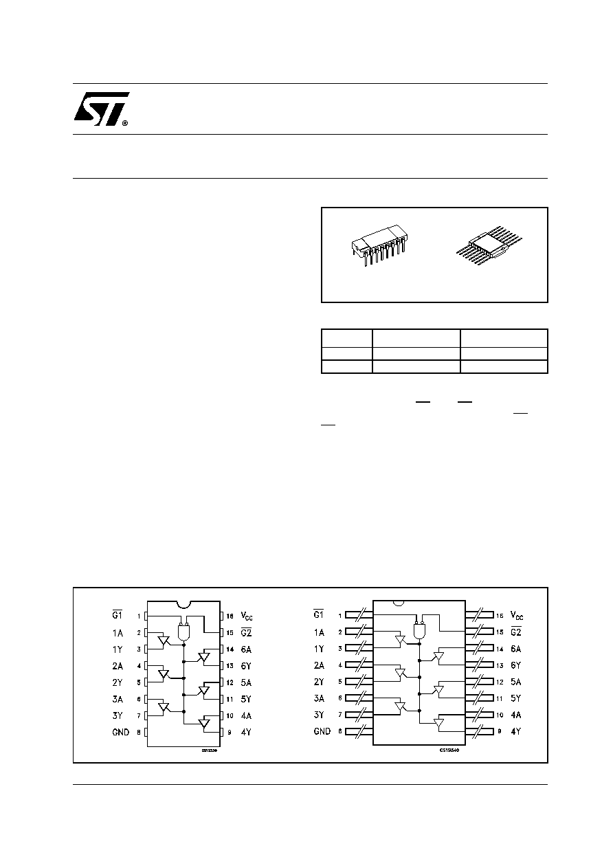
PIN CONNECTION
ORDER CODES
PACKAGE
FM
EM
DILC
M54HC365D
M54HC365D1
FPC
M54HC365K
M54HC365K1
DILC-16
FPC-16
Rev. 1
M54HC365
2/11
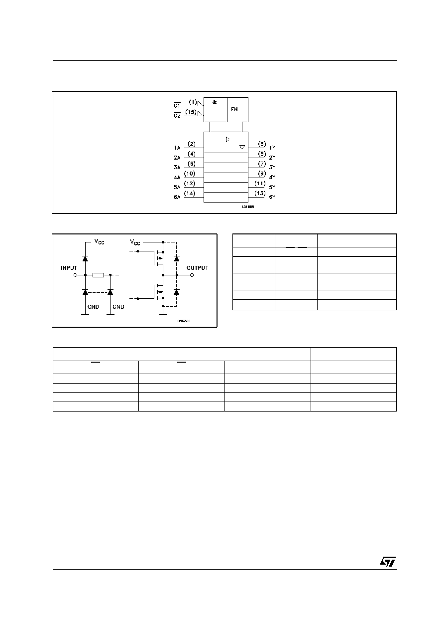
Figure 1: IEC Logic Symbols
Figure 2: Input And Output Equivalent Circuit
Table 1: Pin Description
Table 2: Truth Table
X : Don't Care
Z : High Impedance
PIN N∞
SYMBOL
NAME AND FUNCTION
1, 15
G1, G2
Output Enable Inputs
2, 4, 6, 10,
12, 14
1A to 6A
Data Inputs
3, 5, 7, 9, 11,
13
1Y to 6Y
Data Outputs
8
GND
Ground (0V)
16
V
CC
Positive Supply Voltage
INPUTS
OUTPUTS
G1
G2
An
Y
L
L
L
L
L
L
H
H
H
X
X
Z
X
H
X
Z
M54HC365
3/11
Table 3: Absolute Maximum Ratings
Absolute Maximum Ratings are those values beyond which damage to the device may occur. Functional operation under these conditions is
not implied
Table 4: Recommended Operating Conditions
Symbol
Parameter
Value
Unit
V
CC
Supply Voltage
-0.5 to +7
V
V
I
DC Input Voltage
-0.5 to V
CC
+ 0.5
V
V
O
DC Output Voltage
-0.5 to V
CC
+ 0.5
V
I
IK
DC Input Diode Current
±
20
mA
I
OK
DC Output Diode Current
±
20
mA
I
O
DC Output Current
±
35
mA
I
CC
or I
GND
DC V
CC
or Ground Current
±
70
mA
P
D
Power Dissipation
420
mW
T
stg
Storage Temperature
-65 to +150
∞C
T
L
Lead Temperature (10 sec)
265
∞C
Symbol
Parameter
Value
Unit
V
CC
Supply Voltage
2 to 6
V
V
I
Input Voltage
0 to V
CC
V
V
O
Output Voltage
0 to V
CC
V
T
op
Operating Temperature
-55 to 125
∞C
t
r
, t
f
Input Rise and Fall Time
V
CC
= 2.0V
0 to 1000
ns
V
CC
= 4.5V
0 to 500
ns
V
CC
= 6.0V
0 to 400
ns
M54HC365
5/11
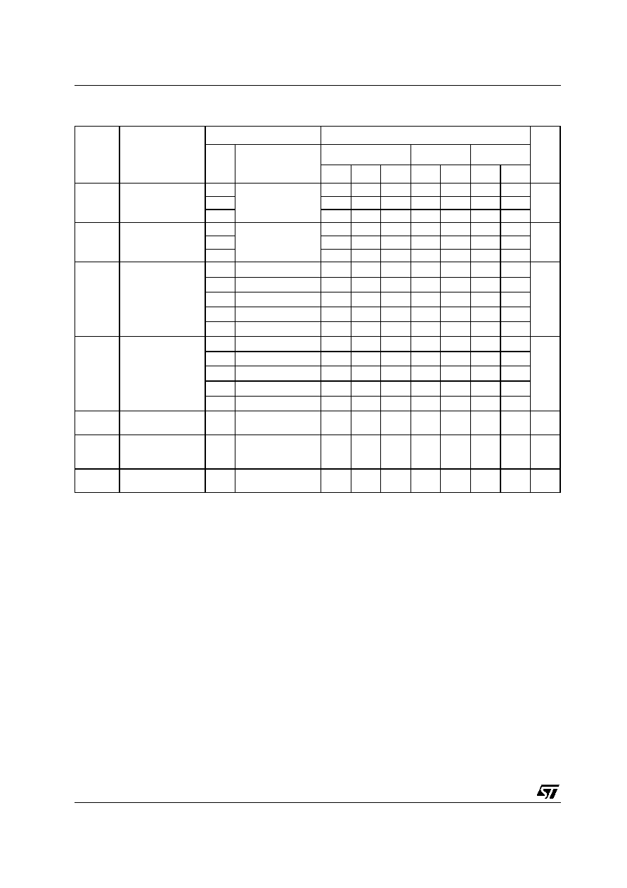
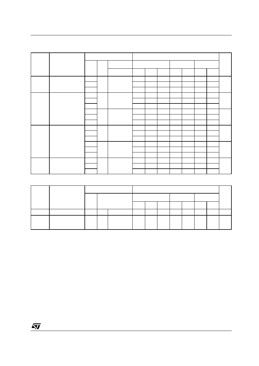
Table 6: AC Electrical Characteristics (C
L
= 50 pF, Input t
r
= t
f
= 6ns)
Table 7: Capacitive Characteristics
1) C
PD
is defined as the value of the IC's internal equivalent capacitance which is calculated from the operating current consumption without
load. (Refer to Test Circuit). Average operating current can be obtained by the following equation. I
CC(opr)
= C
PD
x V
CC
x f
IN
+ I
CC
/6 (per gate)
Symbol
Parameter
Test Condition
Value
Unit
V
CC
(V)
C
L
(pF)
T
A
= 25∞C
-40 to 85∞C
-55 to 125∞C
Min.
Typ.
Max.
Min.
Max.
Min.
Max.
t
TLH
t
THL
Output Transition
Time
2.0
50
25
60
75
90
ns
4.5
7
12
19
18
6.0
6
10
13
15
t
PLH
t
PHL
Propagation Delay
Time
2.0
50
38
90
115
135
ns
4.5
12
18
23
27
6.0
10
15
20
23
2.0
150
51
130
165
195
ns
4.5
17
26
33
39
6.0
14
22
28
33
t
PZL
t
PZH
High Impedance
Output Enable
Time
2.0
50
R
L
= 1 K
64
130
165
195
ns
4.5
16
26
33
39
6.0
14
22
28
33
2.0
150
R
L
= 1 K
76
150
190
225
ns
4.5
19
30
38
45
6.0
16
26
32
38
t
PLZ
t
PHZ
High Impedance
Output Disable
Time
2.0
50
R
L
= 1 K
42
130
165
195
ns
4.5
18
26
33
39
6.0
15
22
28
33
Symbol
Parameter
Test Condition
Value
Unit
V
CC
(V)
T
A
= 25∞C
-40 to 85∞C
-55 to 125∞C
Min.
Typ.
Max.
Min.
Max.
Min.
Max.
C
IN
Input Capacitance
5.0
5
10
10
10
pF
C
PD
Power Dissipation
Capacitance (note
1)
5.0
27
pF