
M54/M74HC367
M54/M74HC368
October 1992
HC367 NON INVERTING, HC368 INVERTING
HEX BUS BUFFER (3-STATE)
B1R
(Plastic Package)
ORDER CODES :
M54HCXXXF1R
M74HCXXXM1R
M74HCXXXB1R
M74HCXXXC1R
F1R
(Ceramic Package)
M1R
(Micro Package)
C1R
(Chip Carrier)
PIN CONNECTIONS (top view)
HC368
HC367
DESCRIPTION
.
HIGH SPEED
t
PD
= 11 ns (TYP.) AT V
CC
= 5 V
.
LOW POWER DISSIPATION
I
CC
= 4
µ
A (MAX.) AT T
A
= 25
∞
C
.
HIGH NOISE IMMUNITY
V
NIH
= V
NIL
= 28 % V
CC
(MIN.)
.
OUTPUT DRIVE CAPABILITY
15 LSTTL LOADS
.
SYMMETRICAL OUTPUT IMPEDANCE
|I
OH
| = I
OL
= 6 mA (MIN.)
.
BALANCED PROPAGATION DELAYS
t
PLH
= t
PHL
.
WIDE OPERATING VOLTAGE RANGE
V
CC
(OPR) = 2 V TO 6 V
.
PIN AND FUNCTION COMPATIBLE WITH
54/74LS367/368
The M54/74HC367 and the M54/74HC368 are high
speed CMOS HEX BUS BUFFER (3-STATE) fabri-
cated in silicon gate C
2
MOS technology. They have
the same high speed performance of LSTTL com-
bined with true CMOS low power consumption.
These devices contain six buffers, four buffers are
controlled by an enable input (G1) and the other two
buffers are controlled by the other enable input
(G2) ; the outputs of each buffer group are enabled
when G1 and/or G2 inputs are held low, and
when held high these outputs are disabled to be
high-impedance.
These outputs are capable of driving up to 15 LSTTL
loads. The designer has a choice of non-inverting
outputs (HC367) and inverting outputs (HC368).
All inputs are equipped with protection circuits
against static discharge and transient excess volt-
age.
1/11
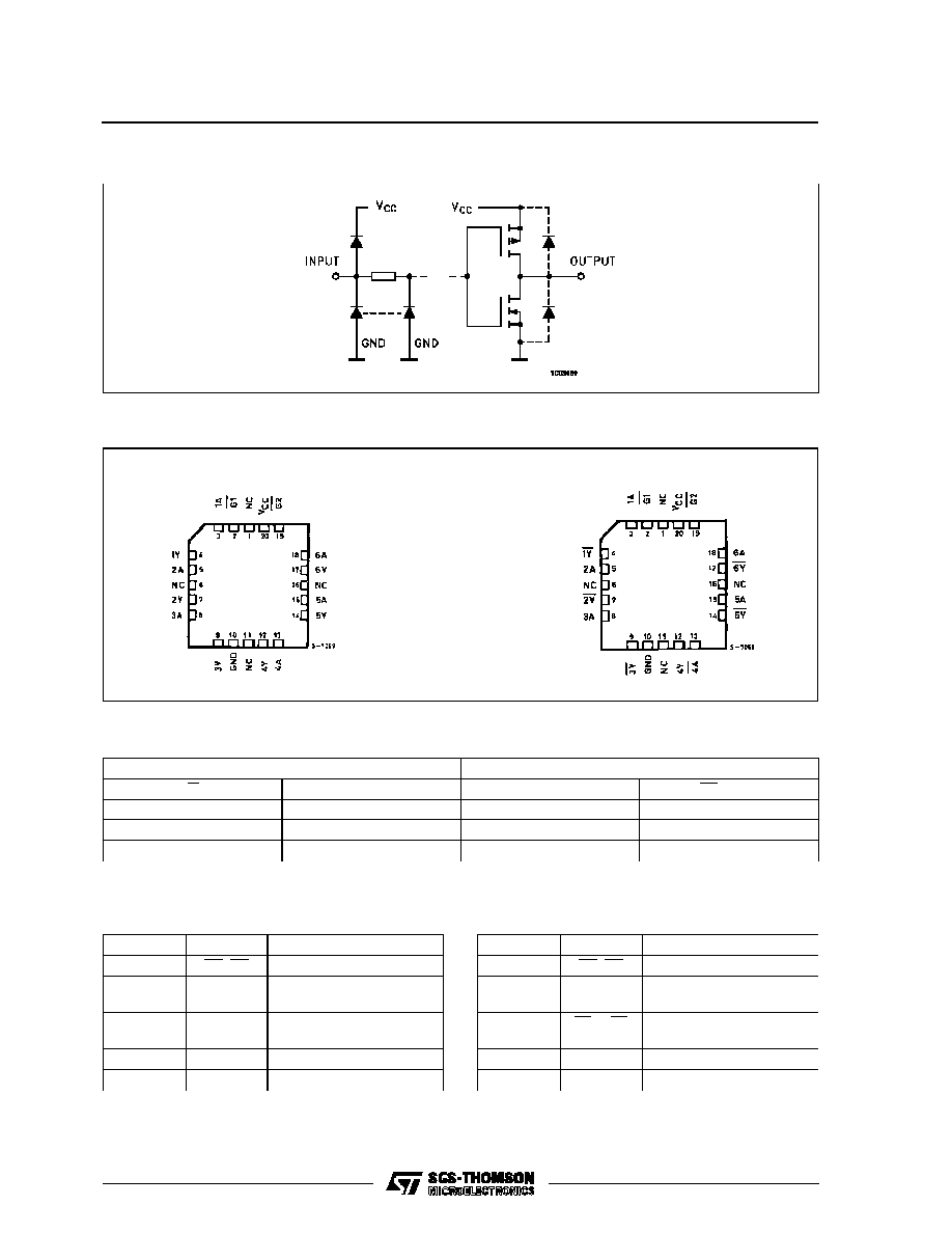
INPUT AND OUTPUT EQUIVALENT CIRCUIT
CHIP CARRIER
NC = No Internal Connection
HC367
HC368
PIN DESCRIPTION (HC367)
PIN No
SYMBOL
NAME AND FUNCTION
1, 15
G1, G2
Output Enable Inputs
2, 4, 6, 10,
12, 14
1A to 6A
Data Inputs
3, 5, 7, 9,
11, 13
1Y to 6Y
Data Outputs
8
GND
Ground (0V)
16
V
CC
Positive Supply Voltage
PIN DESCRIPTION (HC368)
PIN No
SYMBOL
NAME AND FUNCTION
1, 15
G1, G2
Output Enable Inputs
2, 4, 6, 10,
12, 14
1A to 6A
Data Inputs
3, 5, 7, 9,
11, 13
1Y to 6Y
Data Outputs
8
GND
Ground (0V)
16
V
CC
Positive Supply Voltage
TRUTH TABLE
INPUTS
OUTPUTS
G
An
Y n (367)
Yn (368)
L
L
L
H
L
H
H
L
H
X
Z
Z
X = DON'T CARE Z = HIGH IMPEDANCE
M54/M74HC367/368
2/11

IEC LOGIC SYMBOL
ABSOLUTE MAXIMUM RATINGS
Symbol
Parameter
Value
Unit
V
CC
Supply Voltage
-0.5 to +7
V
V
I
DC Input Voltage
-0.5 to V
CC
+ 0.5
V
V
O
DC Output Voltage
-0.5 to V
CC
+ 0.5
V
I
IK
DC Input Diode Current
±
20
mA
I
OK
DC Output Diode Current
±
20
mA
I
O
DC Output Source Sink Current Per Output Pin
±
35
mA
I
CC
or I
GND
DC V
CC
or Ground Current
±
70
mA
P
D
Power Dissipation
500 (*)
mW
T
stg
Storage Temperature
-65 to +150
o
C
T
L
Lead Temperature (10 sec)
300
o
C
Absolute Maximum Ratings are those values beyond which damage to the device may occur. Functional operation under these condition is not implied.
(*) 500 mW:
65
o
C derate to 300 mW by 10mW/
o
C: 65
o
C to 85
o
C
RECOMMENDED OPERATING CONDITIONS
Symbol
Parameter
Value
Unit
V
CC
Supply Voltage
2 to 6
V
V
I
Input Voltage
0 to V
CC
V
V
O
Output Voltage
0 to V
CC
V
T
op
Operating Temperature: M54HC Series
M74HC Series
-55 to +125
-40 to +85
o
C
o
C
t
r
, t
f
Input Rise and Fall Time
V
CC
= 2 V
0 to 1000
ns
V
CC
= 4.5 V
0 to 500
V
CC
= 6 V
0 to 400
HC367
HC368
M54/M74HC367/368
3/11

DC SPECIFICATIONS
Symbol
Parameter
Test Conditions
Value
Unit
V
CC
(V)
T
A
= 25
o
C
54HC and 74HC
-40 to 85
o
C
74HC
-55 to 125
o
C
54HC
Min.
Typ.
Max.
Min.
Max.
Min.
Max.
V
IH
High Level Input
Voltage
2.0
1.5
1.5
1.5
V
4.5
3.15
3.15
3.15
6.0
4.2
4.2
4.2
V
IL
Low Level Input
Voltage
2.0
0.5
0.5
0.5
V
4.5
1.35
1.35
1.35
6.0
1.8
1.8
1.8
V
OH
High Level
Output Voltage
2.0
V
I
=
V
IH
or
V
IL
I
O
=-20
µ
A
1.9
2.0
1.9
1.9
V
4.5
4.4
4.5
4.4
4.4
6.0
5.9
6.0
5.9
5.9
4.5
I
O
=-6.0 mA
4.18
4.31
4.13
4.10
6.0
I
O
=-7.8 mA
5.68
5.8
5.63
5.60
V
OL
Low Level Output
Voltage
2.0
V
I
=
V
IH
or
V
IL
I
O
= 20
µ
A
0.0
0.1
0.1
0.1
V
4.5
0.0
0.1
0.1
0.1
6.0
0.0
0.1
0.1
0.1
4.5
I
O
= 6.0 mA
0.17
0.26
0.33
0.40
6.0
I
O
= 7.8 mA
0.18
0.26
0.33
0.40
I
I
Input Leakage
Current
6.0
V
I
= V
CC
or GND
±
0.1
±
1
±
1
µ
A
I
OZ
3 State Output
Off State Current
6.0
V
I
= V
IH
or V
IL
V
O
= V
CC
or GND
±
0.5
±
5
±
10
µ
A
I
CC
Quiescent Supply
Current
6.0
V
I
= V
CC
or GND
4
40
80
µ
A
M54/M74HC367/368
4/11

AC ELECTRICAL CHARACTERISTICS (C
L
= 50 pF, Input t
r
= t
f
= 6 ns)
Symbol
Parameter
Test Conditions
Value
Unit
V
CC
(V)
C
L
(pF)
T
A
= 25
o
C
54HC and 74HC
-40 to 85
o
C
74HC
-55 to 125
o
C
54HC
Min.
Typ.
Max.
Min.
Max.
Min.
Max.
t
TLH
t
THL
Output Transition
Time
2.0
50
25
60
75
90
ns
4.5
7
12
15
18
6.0
6
10
13
15
t
PLH
t
PHL
Propagation
Delay Time
2.0
50
30
85
105
130
ns
4.5
10
17
21
26
6.0
9
14
18
22
2.0
150
42
105
130
160
ns
4.5
14
21
26
32
6.0
12
18
22
27
t
PZL
t
PZH
Output Enable
Time
2.0
50
R
L
= 1 K
36
90
115
135
ns
4.5
11
18
23
27
6.0
9
15
20
23
2.0
150
R
L
= 1 K
49
110
140
165
ns
4.5
15
22
28
33
6.0
13
19
24
28
t
PLZ
t
PHZ
Output Disable
Time
2.0
50
R
L
= 1 K
32
95
120
145
ns
4.5
14
19
24
29
6.0
12
16
20
25
C
IN
Input Capacitance
5
10
10
10
pF
C
PD
(*)
Power Dissipation
Capacitance
33
pF
(*) C
PD
is defined as the value of the IC's internal equivalent capacitance which is calculated from the operating current consumption without load.
(Refer to Test Circuit). Average operting current can be obtained by the following equation. I
CC
(opr) = C
PD
∑
V
CC
∑
f
IN
+ I
CC
/6 (per Channel)
TEST CIRCUIT I
CC
(Opr.)
INPUT WAVEFORM IS THE SAME AS THAT IN CASE OF
SWITCHING CHARACTERISTICS TEST.
C
PD
CALCULATION
C
PD
is to be calculated with the following
formula by using the measured value of
I
CC
(opr.) in the test circuit opposite.
C
PD
=
I
CC
(
opr
)
f
IN
◊
V
CC
In determining the typical value of C
PD
, a
relatively high frequency of 1 MHz was ap-
plied to f
IN
, in order to eliminate any error
caused by the quiescent supply current.
M54/M74HC367/368
5/11