M54/74HC373
M54/74HC533
October 1993
HC373 NON INVERTING - HC533 INVERTING
OCTAL D-TYPE LATCH WITH 3 STATE OUTPUT
B1R
(Plastic Package)
ORDER CODES :
M54HCXXXF1R
M74HCXXXM1R
M74HCXXXB1R
M74HCXXXC1R
F1R
(Ceramic Package)
M1R
(Micro Package)
C1R
(Chip Carrier)
PIN CONNECTION (top view)
.
HIGH SPEED
t
PD
= 11 ns (TYP.) AT V
CC
= 5 V
.
LOW POWER DISSIPATION
I
CC
= 4
µ
A (MAX.) AT T
A
= 25
∞
C
.
HIGH NOISE IMMUNITY
V
NIH
= V
NIL
= 28 % V
CC
(MIN.)
.
OUTPUT DRIVE CAPABILITY
15 LSTTL LOADS
.
SYMMETRICAL OUTPUT IMPEDANCE
I
OL
=
I
OH
= 6 mA (MIN.)
.
BALANCED PROPAGATION DELAYS
t
PLH
= t
PHL
.
WIDE OPERATING VOLTAGE RANGE
V
CC
(OPR) = 2 V TO 6 V
.
PIN AND FUNCTION COMPATIBLE
WITH 54/74LS373/533
DESCRIPTION
The M54/74HC373/533 are high speed CMOS
OCTAL
LATCH
WITH
3-STATE
OUTPUTS
fabricated with in silicon gate C
2
MOS technology.
These ICs achive the high speed operation similar
to equivalent LSTTL while maintaning the CMOS
low power dissipation.
These 8 bit D-Type latches are controlled by a latch
enable input (LE) and a output enable input (OE).
While the LE input is held at a high level, the Q
outputs will follow the data input precisely or
inversely. When the LE is taken low, the Q outputs
will be latched precisely or inversely at the logic level
of D input data. While the OE input is at low level,
the eight outputs will be in a normal logic state (high
or low logic level) and while high level the outpts will
be in a high impedance state.
The
application
designer
has
a
choise
of
combination of inverting and non inverting outputs.
The three state output configuration and the wide
choise of outline make bus organized system
simple.
All inputs are equipped with protection circuits
against discharge and transient excess voltage.
HC373
HC533
HC373
HC533
1/13
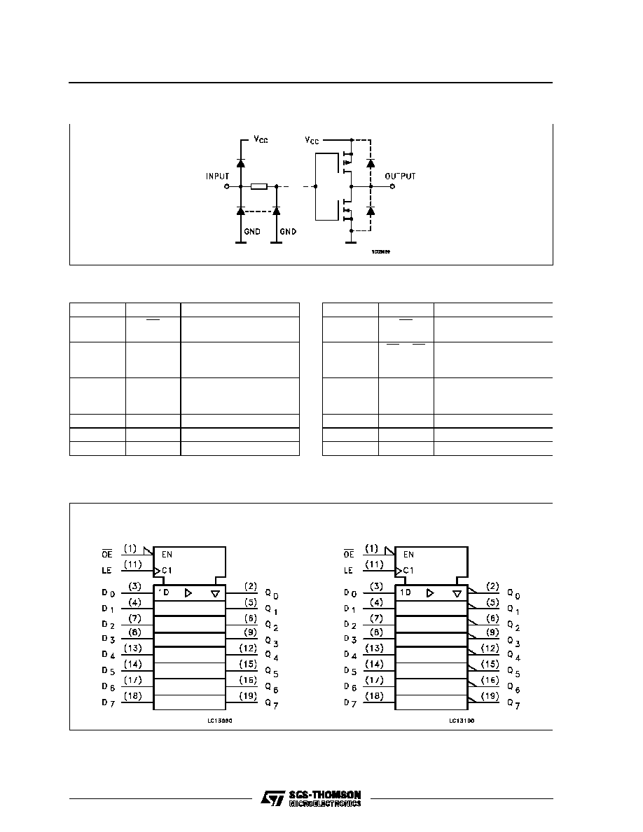
INPUT AND OUTPUT EQUIVALENT CIRCUIT
PIN DESCRIPTION (HC373)
PIN No
SYMBOL
NAME AND FUNCTION
1
OE
3 State output Enable
Input (Active LOW)
2, 5, 6, 9,
12, 15, 16,
19
Q0 to Q7
3 State outputs
3, 4, 7, 8,
13, 14, 17,
18
D0 to D7
Data Inputs
11
LE
Latch Enable Input
10
GND
Ground (0V)
20
V
CC
Positive Supply Voltage
PIN DESCRIPTION (HC533)
PIN No
SYMBOL
NAME AND FUNCTION
1
OE
3 State output Enable
Input (Active LOW)
2, 5, 6, 9,
12, 15, 16,
19
Q0 to Q7
3 State outputs
3, 4, 7, 8,
13, 14, 17,
18
D0 to D7
Data Inputs
11
LE
Latch Enable Input
10
GND
Ground (0V)
20
V
CC
Positive Supply Voltage
IEC LOGIC SYMBOLS
HC373
HC533
M54/M74HC373/533
2/13

ABSOLUTE MAXIMUM RATINGS
Symbol
Parameter
Value
Unit
V
CC
Supply Voltage
-0.5 to +7
V
V
I
DC Input Voltage
-0.5 to V
CC
+ 0.5
V
V
O
DC Output Voltage
-0.5 to V
CC
+ 0.5
V
I
IK
DC Input Diode Current
±
20
mA
I
OK
DC Output Diode Current
±
20
mA
I
O
DC Output Source Sink Current Per Output Pin
±
35
mA
I
CC
or I
GND
DC V
CC
or Ground Current
±
70
mA
P
D
Power Dissipation
500 (*)
mW
T
stg
Storage Temperature
-65 to +150
o
C
T
L
Lead Temperature (10 sec)
300
o
C
Absolute Maximum Ratings are those values beyond which damage tothe device may occur. Functional operation under these conditions is not implied.
(*) 500 mW:
65
o
C derate to 300 mW by 10mW/
o
C: 65
o
C to 85
o
C
RECOMMENDED OPERATING CONDITIONS
Symbol
Parameter
Value
Unit
V
CC
Supply Voltage
2 to 6
V
V
I
Input Voltage
0 to V
CC
V
V
O
Output Voltage
0 to V
CC
V
T
op
Operating Temperature:
M54HC Series
M74HC Series
-55 to +125
-40 to +85
o
C
o
C
t
r
, t
f
Input Rise and Fall Time
V
CC
= 2 V
0 to 1000
ns
V
CC
= 4.5 V
0 to 500
V
CC
= 6 V
0 to 400
M54/M74HC373/533
4/13