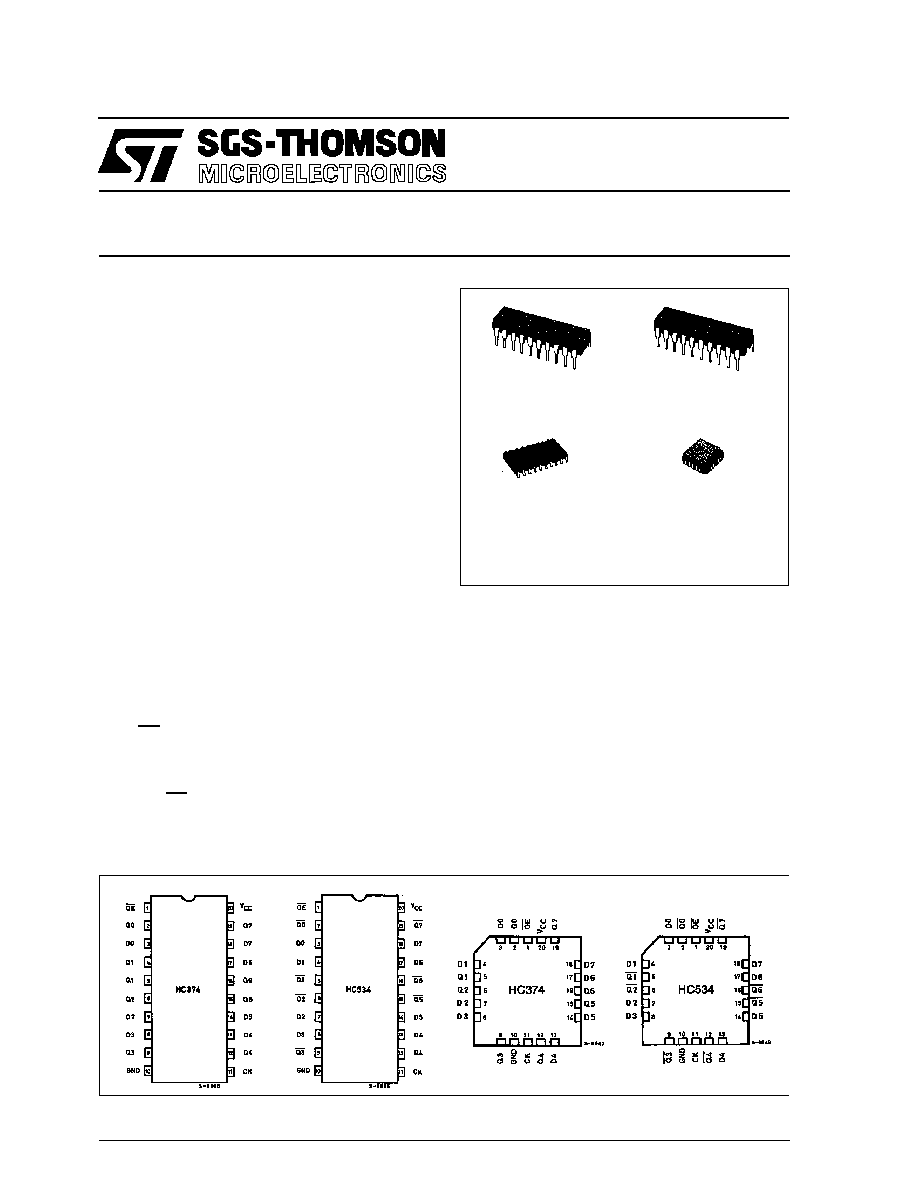
M54/74HC374
M54/74HC534
March 1993
HC374 NON INVERTING - HC534 INVERTING
OCTAL D-TYPE FLIP FLOP WITH 3 STATE OUTPUT
B1R
(Plastic Package)
ORDER CODES :
M54HCXXXF1R
M74HCXXXM1R
M74HCXXXB1R
M74HCXXXC1R
F1R
(Ceramic Package)
M1R
(Micro Package)
C1R
(Chip Carrier)
PIN CONNECTION (top view)
.
HIGH SPEED
f
MAX
= 77 MHz (TYP.) AT V
CC
= 5 V
.
LOW POWER DISSIPATION
I
CC
= 4
µ
A (MAX.) AT T
A
= 25
∞
C
.
HIGH NOISE IMMUNITY
V
NIH
= V
NIL
= 28 % V
CC
(MIN)
.
OUTPUT DRIVE CAPABILITY
15 LSTTL LOADS
.
SYMMETRICAL OUTPUT IMPEDANCE
I
OL
=
I
OH
= 6 mA (MIN.)
.
BALANCED PROPAGATION DELAYS
t
PLH
= t
PHL
.
WIDE OPERATING VOLTAGE RANGE
V
CC
(OPR) = 2 V TO 6 V
.
PIN AND FUNCTION COMPATIBLE
WITH 54/74LS374/534
DESCRIPTION
The M54/74HC374, M54/74HC534, are high speed
CMOS OCTAL D-TYPE FLIP FLOP WITH 3-STATE
OUTPUTS fabricated with in silicon gate C
2
MOS
technology. They have the same high speed per-
formance of LSTTL combined with true CMOS low
power comsuption. These8-bit D-type flip-flops are
controlled by a clock input (CK) and an ouput enable
input (OE). On the positive transition of the clock, the
Q outputs will be set to the logic state that were setup
at the D inputs (HC374) or their complements
(HC534).
While the OE input is low, the eight outputs will be
in a normal logic state (high or low logic level), and
while high level, the outputs will be in a high imped-
ance state. The output control does not affect the in-
ternal operation of flip-flops. That is, the old data can
be retained or the new data can be entered even
while the outputs are off. The application engineer
has a choice of combination of inverting and non-in-
verting outputs. The HC374 and HC574 are identi-
cal, apart from pin layout. The 3-state output
configuration and the wide choice of outline make
bus-organized systems simple. All inputs are
equipped with protection circuits against static dis-
charge and transient excess voltage.
1/13

INPUT AND OUTPUT EQUIVALENT CIRCUIT
PIN DESCRIPTION (HC374)
PIN No
SYMBOL
NAME AND FUNCTION
1
OE
3 State output Enable
Input (Active LOW)
2, 5, 6, 9,
12, 15, 16,
19
Q0 to Q7
3 State outputs
3, 4, 7, 8,
13, 14, 17,
18
D0 to D7
Data Inputs
11
CLOCK
Clock Input (LOW to
HIGH, edge triggered)
10
GND
Ground (0V)
20
V
CC
Positive Supply Voltage
PIN DESCRIPTION (HC534)
PIN No
SYMBOL
NAME AND FUNCTION
1
OE
3 State output Enable
Input (Active LOW)
2, 5, 6, 9,
12, 15, 16,
19
Q0 to Q7
3 State outputs
3, 4, 7, 8,
13, 14, 17,
18
D0 to D7
Data Inputs
11
CLOCK
Clock Input (LOW to
HIGH, edge triggered)
10
GND
Ground (0V)
20
V
CC
Positive Supply Voltage
IEC LOGIC SYMBOLS
HC374
HC534
M54/M74HC374/534
2/13
ABSOLUTE MAXIMUM RATINGS
Symbol
Parameter
Value
Unit
V
CC
Supply Voltage
-0.5 to +7
V
V
I
DC Input Voltage
-0.5 to V
CC
+ 0.5
V
V
O
DC Output Voltage
-0.5 to V
CC
+ 0.5
V
I
IK
DC Input Diode Current
±
20
mA
I
OK
DC Output Diode Current
±
20
mA
I
O
DC Output Source Sink Current Per Output Pin
±
35
mA
I
CC
or I
GND
DC V
CC
or Ground Current
±
70
mA
P
D
Power Dissipation
500 (*)
mW
T
stg
Storage Temperature
-65 to +150
o
C
T
L
Lead Temperature (10 sec)
300
o
C
Absolute Maximum Ratings are those values beyond which damage to the device may occur. Functional operation under these condition is not implied.
(*) 500 mW:
65
o
C derate to 300 mW by 10mW/
o
C: 65
o
C to 85
o
C
RECOMMENDED OPERATING CONDITIONS
Symbol
Parameter
Value
Unit
V
CC
Supply Voltage
2 to 6
V
V
I
Input Voltage
0 to V
CC
V
V
O
Output Voltage
0 to V
CC
V
T
op
Operating Temperature:
M54HC Series
M74HC Series
-55 to +125
-40 to +85
o
C
o
C
t
r
, t
f
Input Rise and Fall Time
V
CC
= 2 V
0 to 1000
ns
V
CC
= 4.5 V
0 to 500
V
CC
= 6 V
0 to 400
M54/M74HC374/534
4/13