M54HC390
M74HC390
February 1993
DUAL DECADE COUNTER
B1R
(Plastic Package)
ORDER CODES :
M54HC390F1R
M74HC390M1R
M74HC390B1R
M74HC390C1R
F1R
(Ceramic Package)
M1R
(Micro Package)
C1R
(Chip Carrier)
PIN CONNECTIONS (top view)
NC =
No Inter-
nal Con-
DESCRIPTION
.
HIGH SPEED
f
MAX
= 84 MHz (TYP.) AT V
CC
= 5 V
.
LOW POWER DISSIPATION
I
CC
= 4
�
A (MAX.) AT T
A
= 25
�
C
.
HIGH NOISE IMMUNITY
V
NIH
= V
NIL
= 28 % V
CC
(MIN.)
.
OUTPUT DRIVE CAPABILITY
10 LSTTL LOADS
.
SYMMETRICAL OUTPUT IMPEDANCE
|I
OH
| = I
OL
= 4 mA (MIN.)
.
BALANCED PROPAGATION DELAYS
t
PLH
= t
PHL
.
WIDE OPERATING VOLTAGE RANGE
V
CC
(OPR) = 2 V TO 6 V
.
PIN AND FUNCTION COMPATIBLE WITH
54/74LS390
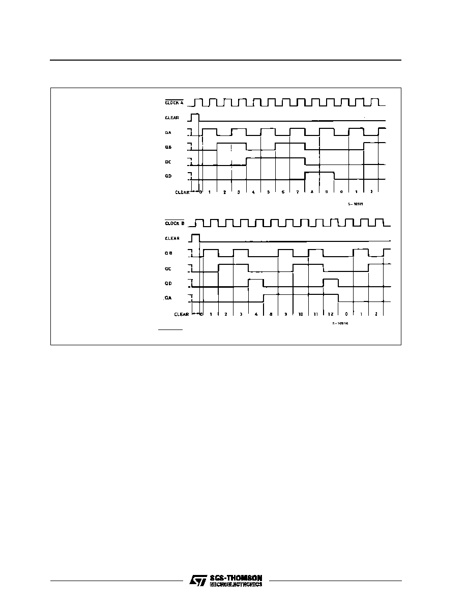
The M54/74HC390 is a high speed CMOS DUAL
DECADE COUNTER fabricated in silicon gate
C
2
MOS technology. It has the same high speed per-
formance of LSTTL combined with true CMOS low
power consumption.
This dual decade counter contains two independent
ripple carry counters. Each counter is composed of
a divide-by-two and divide-by-five counter. The
divide-by-two and divide-by-five counters can be
cascaded to form dual decade, dual biquinary, or
various combinations up to a single divide-by-100
counter.
Each 4-bit counter is incremented on the high to low
transition (negative edge) of the clock input, and
each has an independent clear input. When clear is
set low all four bits of each counter are set to low.
This enables count truncation and allows the im-
plementation of divide-by-N counter configurations.
All inputs are equipped with protection circuits
against static discharge and transient excess volt-
age.
1/13

TRUTH TABLE
COUNT
OUTPUTS
BCD COUNT *
BI-QUINARY **
QD
QC
QB
QA
QA
QD
QC
QB
0
L
L
L
L
L
L
L
L
1
L
L
L
H
L
L
L
H
2
L
L
H
L
L
L
H
L
3
L
L
H
H
L
L
H
H
4
L
H
L
L
L
H
L
L
5
L
H
L
H
H
L
L
L
6
L
H
H
L
H
L
L
H
7
L
H
H
H
H
L
H
L
8
H
L
L
L
H
L
H
H
9
H
L
L
H
H
H
L
L
INPUTS
OUTPUTS
CLOCK A
CLOCK B
CLEAR
QA
QB
QC
QD
X
X
H
L
L
L
L
X
L
BINARY COUNT UP
X
L
QUINARY COUNT UP
Note: * Output QA is connected to input CLOCK B for BCD count.
** Output QD is connected to input CLOCK A for bi-quinary count.
INPUT AND OUTPUT EQUIVALENT CIRCUIT
M54/M74HC390
2/13

PIN DESCRIPTION
PIN No
SYMBOL
NAME AND FUNCTION
1, 15
1 CLOCK A
2 CLOCK B
Clock Input Divide by 2
Section (HIGH to LOW
Edge-triggered)
2, 14
1 CLEAR
2 CLEAR
Asynchronous Master
Reset Inputs
3, 5, 6, 7
1QA to 1QD
Flip Flop Outputs
4, 12
1 CLOCK B
2 CLOCK B
Clock Input Divide by 5
Section (HIGH to LOW
Edge-triggered)
13, 11, 10, 9 2QA to 2QD
Flip Flop Outputs
8
GND
Ground (0V)
16
V
CC
Positive Supply Voltage
IEC LOGIC SYMBOL
ABSOLUTE MAXIMUM RATINGS
Symbol
Parameter
Value
Unit
V
CC
Supply Voltage
-0.5 to +7
V
V
I
DC Input Voltage
-0.5 to V
CC
+ 0.5
V
V
O
DC Output Voltage
-0.5 to V
CC
+ 0.5
V
I
IK
DC Input Diode Current
�
20
mA
I
OK
DC Output Diode Current
�
20
mA
I
O
DC Output Source Sink Current Per Output Pin
�
25
mA
I
CC
or I
GND
DC V
CC
or Ground Current
�
50
mA
P
D
Power Dissipation
500 (*)
mW
T
stg
Storage Temperature
-65 to +150
o
C
T
L
Lead Temperature (10 sec)
300
o
C
Absolute Maximum Ratings are those values beyond which damage to the device may occur. Functional operation under these condition is not implied.
(*) 500 mW:
65
o
C derate to 300 mW by 10mW/
o
C: 65
o
C to 85
o
C
RECOMMENDED OPERATING CONDITIONS
Symbol
Parameter
Value
Unit
V
CC
Supply Voltage
2 to 6
V
V
I
Input Voltage
0 to V
CC
V
V
O
Output Voltage
0 to V
CC
V
T
op
Operating Temperature: M54HC Series
M74HC Series
-55 to +125
-40 to +85
o
C
o
C
t
r
, t
f
Input Rise and Fall Time
V
CC
= 2 V
0 to 1000
ns
V
CC
= 4.5 V
0 to 500
V
CC
= 6 V
0 to 400
M54/M74HC390
5/13