1/16
September 2001
s
HIGH SPEED :
f
MAX
= 38MHz (TYP.) at V
CC
= 6V
s
LOW POWER DISSIPATION:
I
CC
=4
µ
A(MAX.) at T
A
=25∞C
s
HIGH NOISE IMMUNITY:
V
NIH
= V
NIL
= 28 % V
CC
(MIN.)
s
SYMMETRICAL OUTPUT IMPEDANCE:
|I
OH
| = I
OL
= 4mA (MIN)
s
BALANCED PROPAGATION DELAYS:
t
PLH
t
PHL
s
WIDE OPERATING VOLTAGE RANGE:
V
CC
(OPR) = 2V to 6V
s
PIN AND FUNCTION COMPATIBLE WITH
74 SERIES 40103
DESCRIPTION
The M74HC40103 is an high speed CMOS
8-STAGE PRESETTABLE SYNCHRONOUS
DOWN COUNTER fabricated with silicon gate
C
2
MOS technology.
The HC40103 consists of an 8 stage synchronous
down counter with a single output which is active
when the internal count is zero. The HC40103
contains a single 8-bit binary counter. This device
has control inputs for enabling or disabling the
clock, for clearing the counter to its maximum
count, and for presetting the counter either
synchronously or asynchronously. All control
inputs and the CARRY-OUT / ZERO DETECT
output are active low logic. In normal operation the
counter is decremented by one count on each
positive transition of the CLOCK. Counting is
inhibited when the CARRY-IN / COUNTER
ENABLE (CI/CE) input is high. The CARRY-OUT /
ZERO-DETECT (CO/ZD) output goes low when
the count reaches zero if the CI/CE input is low,
and remains low for one full clock period. When
the SYNCHRONOUS PRESET-ENABLE (SPE)
input is low, data at the J input is clocked into the
counter on the next positive clock transition
regardless of the state of the CI/CE input.
When the ASYNCHRONOUS PRESET-ENABLE
(APE) input is low, data at the J inputs is
asynchronously forced into the counter regardless
of the state of the SPE CI/CE or CLOCK inputs. J
input J0-J7 represent a singular 8-bit binary word.
When the CLEAR, CLR input is low, the counter is
asynchronously cleared to its maximum count
M74HC40103
8 STAGE PRESETTABLE
SYNCHRONOUS DOWN COUNTER
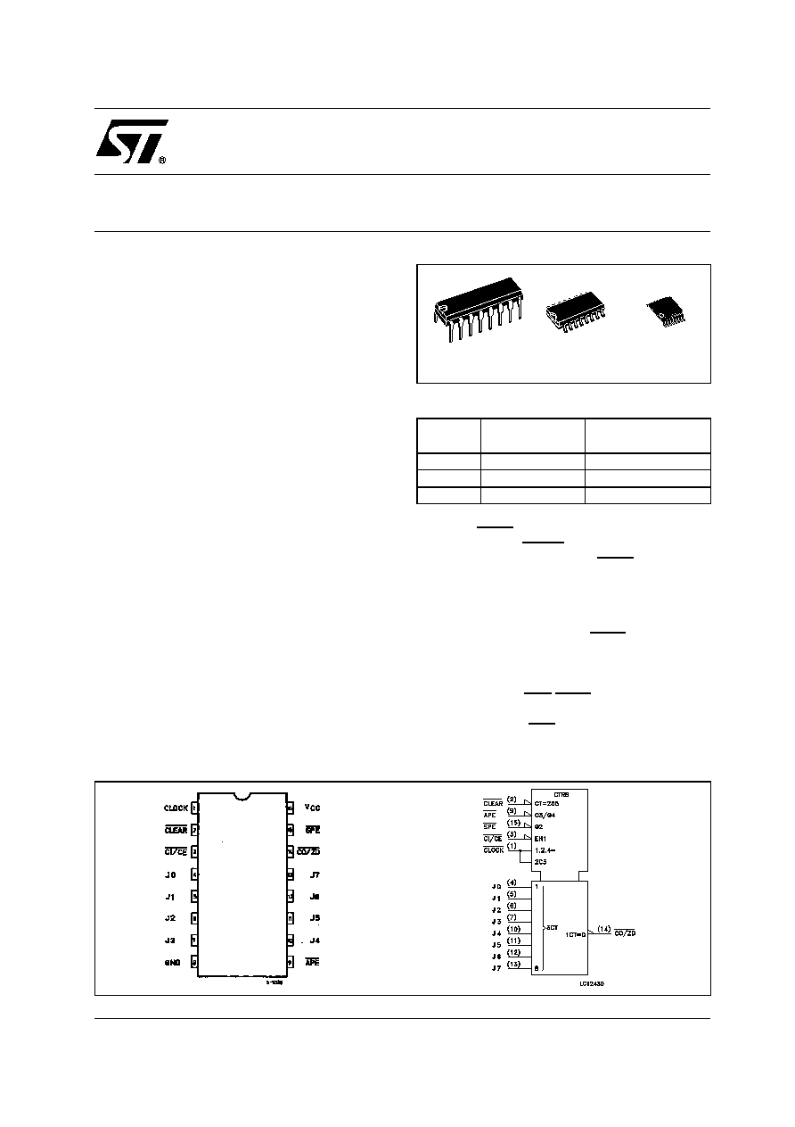
PIN CONNECTION AND IEC LOGIC SYMBOLS
ORDER CODES
PACKAG
E
TUBE
T & R
DIP
M74HC40103B1R
SOP
M74HC40103M1R M74HC40103RM13TR
TSSOP
M74HC40103TTR
TSSOP
DIP
SOP

M74HC40103
2/16
(255
10
) regardless of the state of any other input.
The precedence relationship between control
input is indicated in the truth table. If all control
inputs are high at the time of zero count, the
counters will jump to the maximum count giving a
INPUT AND OUTPUT EQUIVALENT CIRCUIT
counting sequence of 256 clock pulses long. The
HC40103 may be cascaded using the CI/CE input
and the CO/ZD output, in either a synchronous or
ripple mode. All inputs are equipped with
protection circuits against static discharge and
transient excess voltage.
PIN DESCRIPTION
TRUTH TABLE
X : Don't Care
Maximum Count is "255"
PIN No
SYMBOL
NAME AND FUNCTION
1
CLOCK
Clock Input (LOW to
HIGH edge triggered)
2
CLEAR
Asynchronous Master
Reset Input (Active Low)
3
CI/CE
Terminal Enable Input
4, 5, 6, 7, 10,
11, 12, 13
J0 to J9
Jam Inputs
9
APE
Asynchronous Preset
Enable Inputs(Active Low)
14
CO/ZD
Terminal Count Output
(Active Low)
15
SPE
Synchronous Preset
Enable Input (Active Low)
8
GND
Ground (0V)
16
Vcc
Positive Supply Voltage
CONTROL INPUTS
MODE
FUNCTIONAL DESCRIPTION
CLEAR
APE
SPE
CI/CE
H
H
H
H
COUNT INHIBIT
EVEN IF CLOCK IS GIVEN, NO COUNT IS MADE
H
H
H
L
REGULAR COUNT
DOWN COUNT AT RISING EDGE OF CLOCK
H
H
L
X
SYNCHRONOUS
PRESET
DATA OF PI TERMINAL IS PRESET AT RISING
EDGE OF CLOCK
H
L
X
X
ASYNCHRONOUS
PRESET
DATA OF PI TERMINAL IS ASYNCHRONOUSLY
PRESET TO CLOCK
L
X
X
X
CLEAR
COUNTER IS SET TO MAXIMUM COUNT
M74HC40103
3/16
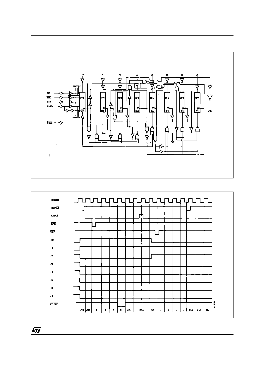
LOGIC DIAGRAM
TIMING CHART

M74HC40103
4/16
ABSOLUTE MAXIMUM RATINGS
Absolute Maximum Ratings are those values beyond which damage to the device may occur. Functional operation under these conditions is
not implied
(*) 500mW at 65
∞
C; derate to 300mW by 10mW/
∞
C from 65
∞
C to 85
∞
C
RECOMMENDED OPERATING CONDITIONS
Symbol
Parameter
Value
Unit
V
CC
Supply Voltage
-0.5 to +7
V
V
I
DC Input Voltage
-0.5 to V
CC
+ 0.5
V
V
O
DC Output Voltage
-0.5 to V
CC
+ 0.5
V
I
IK
DC Input Diode Current
±
20
mA
I
OK
DC Output Diode Current
±
20
mA
I
O
DC Output Current
±
25
mA
I
CC
or I
GND
DC V
CC
or Ground Current
±
50
mA
P
D
Power Dissipation
500(*)
mW
T
stg
Storage Temperature
-65 to +150
∞C
T
L
Lead Temperature (10 sec)
300
∞C
Symbol
Parameter
Value
Unit
V
CC
Supply Voltage
2 to 6
V
V
I
Input Voltage
0 to V
CC
V
V
O
Output Voltage
0 to V
CC
V
T
op
Operating Temperature
-55 to 125
∞C
t
r
, t
f
Input Rise and Fall Time
V
CC
= 2.0V
0 to 1000
ns
V
CC
= 4.5V
0 to 500
ns
V
CC
= 6.0V
0 to 400
ns

M74HC40103
5/16
DC SPECIFICATIONS
AC ELECTRICAL CHARACTERISTICS (C
L
= 50 pF, Input t
r
= t
f
= 6ns)
Symbol
Parameter
Test Condition
Value
Unit
V
CC
(V)
T
A
= 25∞C
-40 to 85∞C
-55 to 125∞C
Min.
Typ.
Max.
Min.
Max.
Min.
Max.
V
IH
High Level Input
Voltage
2.0
1.5
1.5
1.5
V
4.5
3.15
3.15
3.15
6.0
4.2
4.2
4.2
V
IL
Low Level Input
Voltage
2.0
0.5
0.5
0.5
V
4.5
1.35
1.35
1.35
6.0
1.8
1.8
1.8
V
OH
High Level Output
Voltage
2.0
I
O
=-20
µ
A
1.9
2.0
1.9
1.9
V
4.5
I
O
=-20
µ
A
4.4
4.5
4.4
4.4
6.0
I
O
=-20
µ
A
5.9
6.0
5.9
5.9
4.5
I
O
=-4.0 mA
4.18
4.31
4.13
4.10
6.0
I
O
=-5.2 mA
5.68
5.8
5.63
5.60
V
OL
Low Level Output
Voltage
2.0
I
O
=20
µ
A
0.0
0.1
0.1
0.1
V
4.5
I
O
=20
µ
A
0.0
0.1
0.1
0.1
6.0
I
O
=20
µ
A
0.0
0.1
0.1
0.1
4.5
I
O
=4.0 mA
0.17
0.26
0.33
0.40
6.0
I
O
=5.2 mA
0.18
0.26
0.33
0.40
I
I
Input Leakage
Current
6.0
V
I
= V
CC
or GND
±
0.1
±
1
±
1
µ
A
I
CC
Quiescent Supply
Current
6.0
V
I
= V
CC
or GND
4
40
80
µ
A
Symbol
Parameter
Test Condition
Value
Unit
V
CC
(V)
T
A
= 25∞C
-40 to 85∞C
-55 to 125∞C
Min.
Typ.
Max.
Min.
Max.
Min.
Max.
t
TLH
t
THL
Output Transition
Time
2.0
30
75
95
110
ns
4.5
8
15
19
22
6.0
7
13
16
19
t
PLH
t
PHL
Propagation Delay
Time
(CK - CO/ZD)
2.0
96
185
230
280
ns
4.5
24
37
46
56
6.0
20
31
39
47
t
PLH
t
PHL
Propagation Delay
Time
(APE - CO/ZD)
2.0
116
225
280
340
ns
4.5
29
45
56
68
6.0
25
38
48
57
t
PLH
t
PHL
Propagation Delay
Time
(CL - CO/ZD)
2.0
104
200
250
300
ns
4.5
26
40
50
60
6.0
22
34
43
51
t
PLH
t
PHL
Propagation Delay
Time
(CI/CE - CO/ZD)
2.0
48
95
120
145
ns
4.5
12
19
24
29
6.0
10
16
20
24