M54HC4028
M74HC4028
October 1992
BCD TO DECIMAL DECODER
B1R
(Plastic Package)
ORDER CODES :
M54HC4028F1R
M74HC4028M1R
M74HC4028B1R
M74HC4028C1R
F1R
(Ceramic Package)
M1R
(Micro Package)
C1R
(Chip Carrier)
PIN CONNECTIONS (top view)
NC =
No Internal
Connection
DESCRIPTION
.
HIGH SPEED
t
PD
= 18 ns (TYP.) AT V
CC
= 5 V
.
LOW POWER DISSIPATION
I
CC
= 4
µ
A (MAX.) AT T
A
= 25
∞
C
.
HIGH NOISE IMMUNITY
V
NIH
= V
NIL
= 28 % V
CC
(MIN.)
.
OUTPUT DRIVE CAPABILITY
10 LSTTL LOADS
.
SYMMETRICAL OUTPUT IMPEDANCE
|I
OH
| = I
OL
= 4 mA (MIN.)
.
BALANCED PROPAGATION DELAYS
t
PLH
= t
PHL
.
WIDE OPERATING VOLTAGE RANGE
V
CC
(OPR) = 2 V TO 6 V
.
PIN AND FUNCTION COMPATIBLE
WITH 4028B
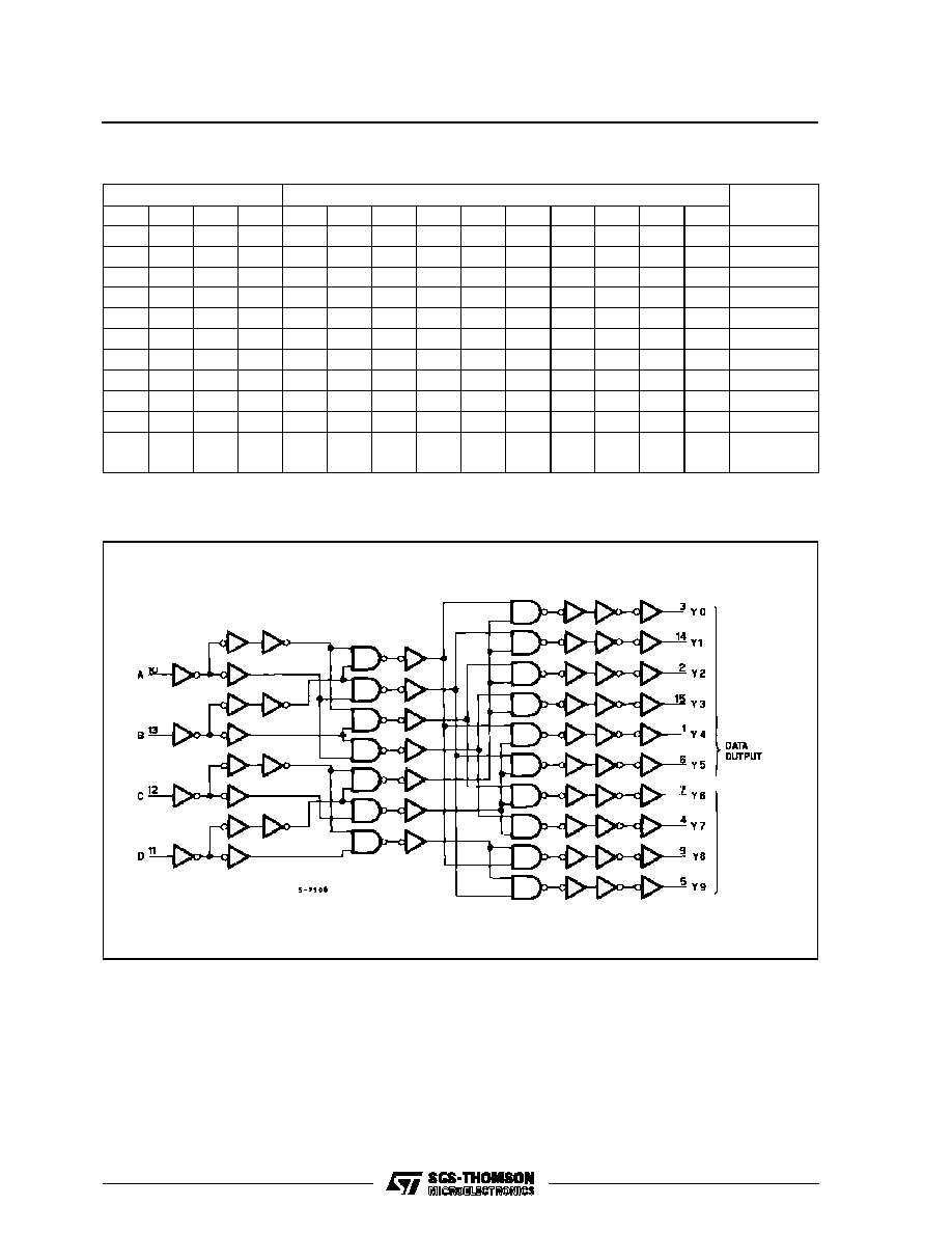
The M54/74HC4028 is a high speed CMOS BCD-
TO-DECIMAL DECODER fabricated in silicon gate
C
2
MOS technology. It has the same high speed per-
formance of LSTTL combined with true CMOS low
power consumption. A BCD code applied to the four
inputs (A to D) provides a high level at the selected
one of the decimal decoded outputs. An illegal BCD
code such as eleven to fifteen gives a low level at
all outputs. The device also can be used as 3-TO-
8-LINE DECODER, when D input is assigned as a
disable input. The device is useful for code conver-
sion, address decoding, memory selection, demulti-
plexing, or read out decoding.
All inputs are equipped with protection circuits
against static discharge and transient excess volt-
age.
1/10

INPUT AND OUTPUT EQUIVALENT CIRCUIT
PIN DESCRIPTION
PIN No
SYMBOL
NAME AND FUNCTION
1, 2, 3, 4, 5,
6, 7, 9, 14,
15
Y0 to Y9
Decoder Outputs
10, 11, 13,
12
A to D
Data Inputs
8
GND
Ground (0V)
16
V
CC
Positive Supply Voltage
IEC LOGIC SYMBOL
ABSOLUTE MAXIMUM RATINGS
Symbol
Parameter
Value
Unit
V
CC
Supply Voltage
-0.5 to +7
V
V
I
DC Input Voltage
-0.5 to V
CC
+ 0.5
V
V
O
DC Output Voltage
-0.5 to V
CC
+ 0.5
V
I
IK
DC Input Diode Current
±
20
mA
I
OK
DC Output Diode Current
±
20
mA
I
O
DC Output Source Sink Current Per Output Pin
±
25
mA
I
CC
or I
GND
DC V
CC
or Ground Current
±
50
mA
P
D
Power Dissipation
500 (*)
mW
T
stg
Storage Temperature
-65 to +150
o
C
T
L
Lead Temperature (10 sec)
300
o
C
Absolute Maximum Ratings are those values beyond which damage to the device may occur. Functional operation under these condition is not implied.
(*) 500 mW:
65
o
C derate to 300 mW by 10mW/
o
C: 65
o
C to 85
o
C
M54/ M74HC4028
3/10

AC ELECTRICAL CHARACTERISTICS (C
L
= 50 pF, Input t
r
= t
f
= 6 ns)
Symbol
Parameter
Test Conditions
Value
Unit
V
CC
(V)
T
A
= 25
o
C
54HC and 74HC
-40 to 85
o
C
74HC
-55 to 125
o
C
54HC
Min.
Typ.
Max.
Min.
Max.
Min.
Max.
t
TLH
t
THL
Output Transition
Time
2.0
30
75
95
110
ns
4.5
8
15
19
22
6.0
7
13
16
19
t
PLH
t
PHL
Propagation
Delay Time
2.0
96
185
230
280
ns
4.5
24
37
46
56
6.0
20
31
39
48
C
IN
Input Capacitance
5
10
10
10
pF
C
PD
(*)
Power Dissipation
Capacitance
39
pF
(*) C
PD
is defined as the value of the IC's internal equivalent capacitance which is calculated from the operating current consumption without load.
(Refer to Test Circuit). Average operting current can be obtained by the following equation. I
CC
(opr) = C
PD
∑
V
CC
∑
f
IN
+ I
CC
SWITCHING CHARACTERISTICS TEST
WAVEFORM
TEST CIRCUIT I
CC
(Opr.)
INPUT TRANSITION TIME IS THE SAME AS THAT IN CASE OF
SWITCHING CHARACTERISTICS TEST.
M54/ M74HC4028
5/10