1/15
May 2004
s
LOW POWER DISSIPATION:
I
CC
= 4
µ
A(MAX.) at T
A
=25∞C
s
LOGIC LEVEL TRANSLATION TO ENABLE
5V LOGIC SIGNAL TO COMMUNICATE
WITH
±
5V ANALOG SIGNAL
s
LOW "ON" RESISTANCE:
70
TYP. (V
CC
- V
EE
= 4.5V)
50
TYP. (V
CC
- V
EE
= 9V)
s
WIDE ANALOG INPUT VOLTAGE RANGE:
±
6V
s
FAST SWITCHING:
t
pd
= 15ns (TYP.) at T
A
= 25 ∞C
s
LOW CROSSTALK BETWEEN SWITCHES
s
HIGH ON/OFF OUTPUT VOLTAGE RATIO
s
WIDE OPERATING SUPPLY VOLTAGE
RANGE (V
CC
- V
EE
) = 2V TO 12V
s
LOW SINE WAVE DISTORTION:
0.02% at V
CC
- V
EE
= 9V
s
HIGH NOISE IMMUNITY:
V
NIH
= V
NIL
= 28% V
CC
(MIN.)
s
PIN AND FUNCTION COMPATIBLE WITH
74 SERIES 4053
DESCRIPTION
The M74HC4053 is a triple two-channel analog
MULTIPLEXER/DEMULTIPLEXER
fabricated
with silicon gate C
2
MOS technology and it is pin to
pin compatible with the equivalent metal gate
CMOS4000B series.
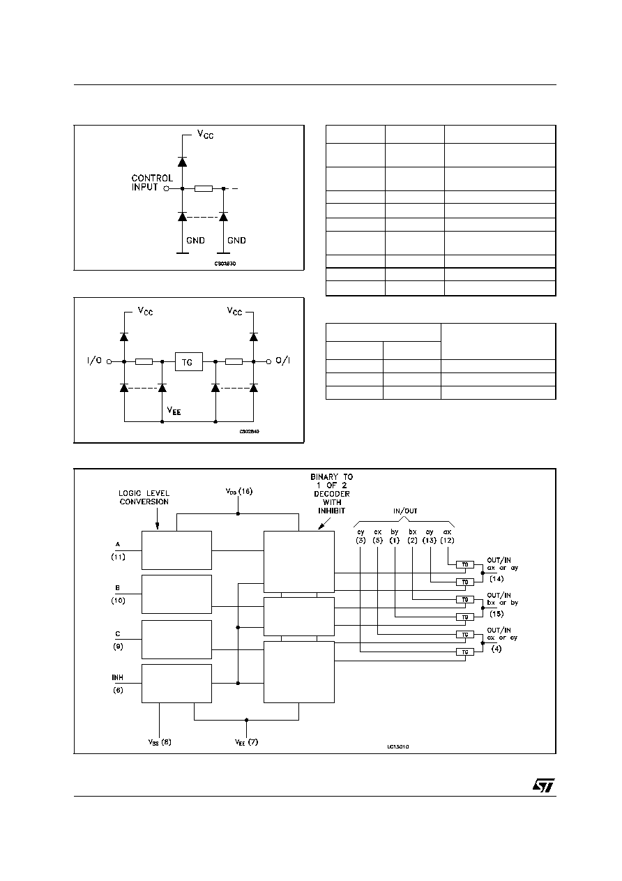
It contains 6 bidirectional and digitally controlled
analog switches.
A built-in level shifting is included to allow an input
range up to
±
6V (peak) for an analog signal with
digital control signal of 0 to 6V.
V
EE
supply pin is provided for analog input
signals. It has an inhibit (INH) input terminal to
disable all the switches when high. For operation
as a digital multiplexer/demultiplexer, VEE is
connected to GND.
A, B and C control inputs select one of a pair of
channels.
All inputs are equipped with protection circuits
against static discharge and transient excess
voltage.
M74HC4053
TRIPLE 2-CHANNEL
ANALOG MULTIPLEXER/DEMULTIPLEXER
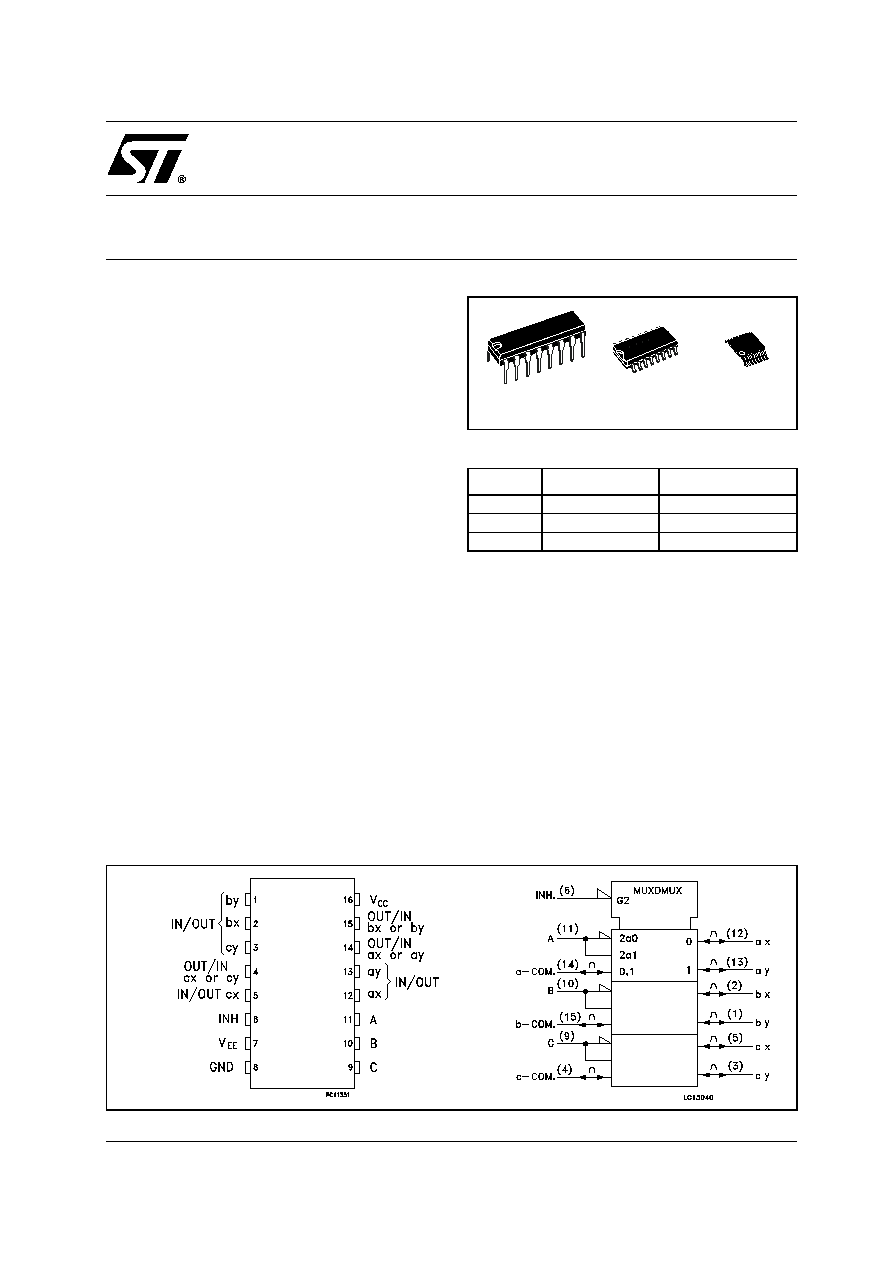
PIN CONNECTION AND IEC LOGIC SYMBOLS
ORDER CODES
PACKAGE
TUBE
T & R
DIP
M74HC4053B1R
SOP
M74HC4053M1R
M74HC4053RM13TR
TSSOP
M74HC4053TTR
TSSOP
DIP
SOP
Rev. 3
M74HC4053
2/15
Figure 1: Control Input Equivalent Circuit
Figure 2: I/O Equivalent Circuit
Table 1: Pin Description
Table 2: Truth Table
X: Don't care
Figure 3: Functional Diagram
PIN N∞
SYMBOL
NAME AND FUNCTION
2, 1
bx, by
Independent Input Out-
puts
5, 3
cx, cy
Independent Input Out-
puts
6
INH
INHIBIT Input
7
V
EE
Negative Supply Voltage
11, 10, 9
A, B, C
Select Inputs
12, 13
ax, ay
Independent Input Out-
puts
14, 15, 4
ax to cy
Common Output/Input
8
GND
Ground (0V)
16
V
CC
Positive Supply Voltage
INPUT STATE
ON CHANNEL
INH
A or B or C
L
L
ax or bx or cx
L
H
ay or by or cy
H
X
NONE

M74HC4053
3/15
Table 3: Absolute Maximum Ratings
Absolute Maximum Ratings are those values beyond which damage to the device may occur. Functional operation under these conditions is
not implied
(*) 500mW at 65
∞
C; derate to 300mW by 10mW/
∞
C from 65
∞
C to 85
∞
C
Table 4: Recommended Operating Conditions
Symbol
Parameter
Value
Unit
V
CC
Supply Voltage
-0.5 to +7
V
V
CC -
V
EE
Supply Voltage
-0.5 to +13
V
V
I
Control Input Voltage
-0.5 to V
CC
+ 0.5
V
V
I/O
Switch I/O Voltage
V
EE
-0.5 to V
CC
+ 0.5
V
I
CK
Control Input Diode Current
±
20
mA
I
IOK
I/O Diode Current
±
20
mA
I
T
Switch Through Current
±
25
mA
I
CC
or I
GND
DC V
CC
or Ground Current
±
50
mA
P
D
Power Dissipation
500(*)
mW
T
stg
Storage Temperature
-65 to +150
∞C
T
L
Lead Temperature (10 sec)
300
∞C
Symbol
Parameter
Value
Unit
V
CC
Supply Voltage
2 to 6
V
V
EE
Supply Voltage
-6 to 0
V
V
CC
- V
EE
Supply Voltage
2 to 12
V
V
I
Input Voltage
0 to V
CC
V
V
I/O
I/O Voltage
V
EE
to V
CC
V
T
op
Operating Temperature
-55 to 125
∞C
t
r
, t
f
Input Rise and Fall Time
V
CC
= 2.0V
0 to 1000
ns
V
CC
= 4.5V
0 to 500
V
CC
= 6.0V
0 to 400

M74HC4053
4/15
Table 5: DC Specifications
Symbol
Parameter
Test Condition
Value
Unit
V
CC
(V)
V
EE
(V)
T
A
= 25∞C
-40 to 85∞C -55 to 125∞C
Min.
Typ.
Max.
Min.
Max.
Min.
Max.
V
IHC
High Level Input
Voltage
2.0
1.5
1.5
1.5
V
4.5
3.15
3.15
3.15
6.0
4.2
4.2
4.2
V
ILC
Low Level Input
Voltage
2.0
0.5
0.5
0.5
V
4.5
1.35
1.35
1.35
6.0
1.8
1.8
1.8
R
ON
ON Resistance
4.5
GND
V
I
= V
IHC
or V
ILC
V
I/O
= V
CC
to V
EE
I
I/O
2mA
85
180
225
270
4.5
-4.5
55
120
150
180
6.0
-6.0
50
100
125
150
2.0
GND
V
I
= V
IHC
or V
ILC
V
I/O
= V
CC
or V
EE
I
I/O
2mA
150
4.5
GND
70
150
190
230
4.5
-4.5
50
100
125
150
6.0
-6.0
45
80
100
120
R
ON
Difference of ON
Resistance
between switches
4.5
GND
V
I
= V
IHC
or V
ILC
V
I/O
= V
CC
or V
EE
I
I/O
2mA
10
30
35
45
4.5
-4.5
5
12
15
18
6.0
-6.0
5
10
12
15
I
OFF
Input/Output
Leakage Current
(SWITCH OFF)
6.0
GND
V
OS
= V
CC
or
GND
V
IS
= GND or V
CC
V
I
= V
ILC
or V
IHC
±
0.06
±
0.6
±
1.2
µ
A
6.0
-6.0
±
0.1
±
1
±
2
I
IZ
Switch Input
Leakage Current
(SWITCH ON,
OUTPUT OPEN)
6.0
GND
V
OS
= V
CC
or
GND
V
I
= V
IHC
or V
ILC
±
0.06
±
0.6
±
1.2
µ
A
6.0
-6.0
±
0.1
±
1
±
2
I
I
Input Leakage
Current
6.0
GND V
I
= V
CC
or GND
±
0.1
±
0.1
±
1
µ
A
I
CC
Quiescent Supply
Current
6.0
GND
V
I
= V
CC
or GND
4
40
80
µ
A
6.0
-6.0
8
80
160

M74HC4053
5/15
Table 6: AC Electrical Characteristics (C
L
= 50 pF, Input t
r
= t
f
= 6ns)
Table 7: Capacitive Characteristics
1) C
PD
is defined as the value of the IC's internal equivalent capacitance which is calculated from the operating current consumption without
load. (Refer to Test Circuit). Average operating current can be obtained by the following equation. I
CC(opr)
= C
PD
x V
CC
x f
IN
+ I
CC
Symbol
Parameter
Test Condition
Value
Unit
V
CC
(V)
V
EE
(V)
T
A
= 25∞C
-40 to 85∞C -55 to 125∞C
Min.
Typ.
Max.
Min.
Max.
Min.
Max.
I/O
Phase Difference
Between Input and
Output
2.0
GND
25
60
75
90
ns
4.5
GND
6
12
15
18
6.0
GND
5
10
13
15
4.5
-4.5
4
t
PZL
t
PZH
Output Enable
Time
2.0
GND
R
L
= 1K
50
225
280
340
ns
4.5
GND
14
45
56
68
6.0
GND
12
38
48
58
4.5
-4.5
14
t
PLZ
t
PHZ
Output Disable
Time
2.0
GND
R
L
= 1K
95
225
280
340
ns
4.5
GND
30
45
56
68
6.0
GND
26
38
48
58
4.5
-4.5
26
Symbol
Parameter
Test Condition
Value
Unit
V
CC
(V)
V
EE
(V)
T
A
= 25∞C
-40 to 85∞C -55 to 125∞C
Min.
Typ.
Max.
Min.
Max.
Min.
Max.
C
IN
Input Capacitance
5.0
5
10
10
10
pF
C
I/O
Common Terminal
Capacitance
5.0
-5.0
11
20
20
20
pF
C
I/O
Switch Terminal
Capacitance
5.0
-5.0
7
15
15
15
pF
C
IOS
Feed Through
Capacitance
5.0
-5.0
0.75
2
2
2
pF
C
PD
Power Dissipation
Capacitance
(note 1)
5.0
GND
67
pF