
M54HC4060
M74HC4060
March 1993
14 STAGE BINARY COUNTER/OSCILLATOR
B1R
(Plastic Package)
ORDER CODES :
M54HC4060F1R
M74HC4060M1R
M74HC4060B1R
M74HC4060C1R
F1R
(Ceramic Package)
M1R
(Micro Package)
C1R
(Chip Carrier)
PIN CONNECTIONS (top view)
NC =
No Internal
Connection
DESCRIPTION
.
HIGH SPEED
f
MAX
= 58 MHz (TYP.) AT V
CC
= 5 V
.
LOW POWER DISSIPATION
I
CC
= 4
µ
A (MAX.) AT T
A
= 25
∞
C
.
HIGH NOISE IMMUNITY
V
NIH
= V
NIL
= 28 % V
CC
(MIN.)
.
OUTPUT DRIVE CAPABILITY
10 LSTTL LOADS
.
SYMMETRICAL OUTPUT IMPEDANCE
|I
OH
| = I
OL
= 4 mA (MIN.)
.
BALANCED PROPAGATION DELAYS
t
PLH
= t
PHL
.
WIDE OPERATING VOLTAGE RANGE
V
CC
(OPR) = 2 V TO 6 V
.
PIN AND FUNCTION COMPATIBLE
WITH 4060B
The M54/74HC4060 is a high speed CMOS 14-
STAGE BINARY COUNTER/OSCILLATOR fabri-
cated in silicon gate C
2
MOS technology. It has the
same high speed performance of LSTTL combined
with true CMOS low power consumption. It operates
ten times faster than metal-gate C
2
MOS IC (4060B)
with the same power dissipation.
The oscillator configuration allows design of either
RC or crystal oscillator circuits. A high level on the
CLEAR accomplishes the reset function, i.e. all
counter outputs are made low and the oscillator is
disabled.
A negative transition on the clock input increments
the counter. Ten kinds of divided output are pro-
vided ; 4 to 10 and 12 to 14 stage inclusive. The
maximum division available at Q12 is 1/16384 f os-
cillator.
The ÿ
1
input and the CLEAR input are equipped
with protection circuits against static discharge and
transient excess voltage.
1/12

INPUT AND OUTPUT EQUIVALENT CIRCUIT
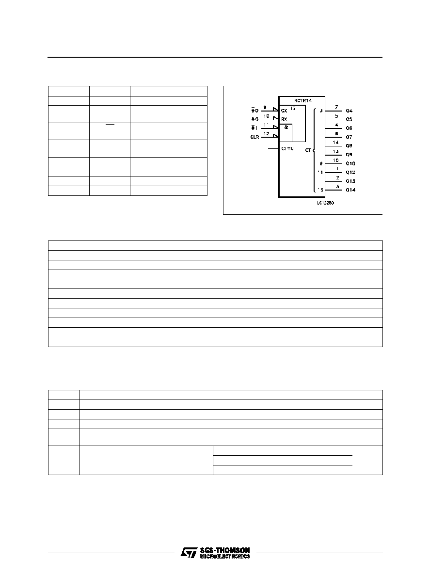
TRUTH TABLE
¯I
CLEAR
FUNCTION
X
H
COUNTER IS RESET TO ZERO STATE
¯0 OUTPUT GOES TO HIGH LEVEL
¯0 OUTPUT GOES TO LOW LEVEL
L
COUNT UP ONE STEP
L
NO CHANGE
X: DON'T CARE
LOGIC DIAGRAM
M54/M74HC4060
2/12
PIN DESCRIPTION
PIN No
SYMBOL
NAME AND FUNCTION
1, 2, 3
Q12 to Q14
Counter Outputs
7, 5, 4, 6,
14, 13, 15
Q4 to Q10
Counter Outputs
9
¯O
External Capacitor
Connection
10
¯O
External Resistor
Connection
11
¯I
Clock Input/Oscillator Pin
12
CLEAR
Master Reset
8
GND
Ground (0V)
16
V
CC
Positive Supply Voltage
IEC LOGIC SYMBOL
ABSOLUTE MAXIMUM RATINGS
Symbol
Parameter
Value
Unit
V
CC
Supply Voltage
-0.5 to +7
V
V
I
DC Input Voltage
-0.5 to V
CC
+ 0.5
V
V
O
DC Output Voltage
-0.5 to V
CC
+ 0.5
V
I
IK
DC Input Diode Current
±
20
mA
I
OK
DC Output Diode Current
±
20
mA
I
O
DC Output Source Sink Current Per Output Pin
±
25
mA
I
CC
or I
GND
DC V
CC
or Ground Current
±
50
mA
P
D
Power Dissipation
500 (*)
mW
T
stg
Storage Temperature
-65 to +150
o
C
T
L
Lead Temperature (10 sec)
300
o
C
Absolute Maximum Ratings are those values beyond which damage to the device may occur. Functional operation under these condition is not implied.
(*) 500 mW:
65
o
C derate to 300 mW by 10mW/
o
C: 65
o
C to 85
o
C
RECOMMENDED OPERATING CONDITIONS
Symbol
Parameter
Value
Unit
V
CC
Supply Voltage
2 to 6
V
V
I
Input Voltage
0 to V
CC
V
V
O
Output Voltage
0 to V
CC
V
T
op
Operating Temperature: M54HC Series
M74HC Series
-55 to +125
-40 to +85
o
C
o
C
t
r
, t
f
Input Rise and Fall Time
V
CC
= 2 V
0 to 1000
ns
V
CC
= 4.5 V
0 to 500
V
CC
= 6 V
0 to 400
M54/ M74HC4060
3/12

DC SPECIFICATIONS
Symbol
Parameter
Test Conditions
Value
Unit
V
CC
(V)
T
A
= 25
o
C
54HC and 74HC
-40 to 85
o
C
74HC
-55 to 125
o
C
54HC
Min.
Typ.
Max.
Min.
Max.
Min.
Max.
V
IH
High Level Input
Voltage
2.0
1.5
1.5
1.5
V
4.5
3.15
3.15
3.15
6.0
4.2
4.2
4.2
V
IL
Low Level Input
Voltage
2.0
0.5
0.5
0.5
V
4.5
1.35
1.35
1.35
6.0
1.8
1.8
1.8
V
OH
High Level
Output Voltage
(Q Outputs)
2.0
V
I
=
V
IH
or
V
IL
I
O
=-20
µ
A
1.9
2.0
1.9
1.9
V
4.5
4.4
4.5
4.4
4.4
6.0
5.9
6.0
5.9
5.9
4.5
I
O
=-4.0 mA
4.18
4.31
4.13
4.10
6.0
I
O
=-5.2 mA
5.68
5.8
5.63
5.60
V
OL
Low Level Output
Voltage
(Q Outputs)
2.0
V
I
=
V
IH
or
V
IL
I
O
= 20
µ
A
0.0
0.1
0.1
0.1
V
4.5
0.0
0.1
0.1
0.1
6.0
0.0
0.1
0.1
0.1
4.5
I
O
= 4.0 mA
0.17
0.26
0.33
0.40
6.0
I
O
= 5.2 mA
0.18
0.26
0.33
0.40
V
OH
High Level
Output Voltage
(¯O, ¯O Output)
2.0
V
I
=
V
IH
or
V
IL
I
O
=-20
µ
A
1.8
2.0
1.8
1.8
V
4.5
4.4
4.5
4.0
4.0
6.0
5.5
5.9
5.5
5.5
V
OL
Low Level Output
Voltage
(¯O, ¯O Output)
2.0
V
I
=
V
IH
or
V
IL
I
O
= 20
µ
A
0.0
0.2
0.2
0.2
V
4.5
0.0
0.5
0.5
0.5
6.0
0.1
0.5
0.5
0.5
I
I
Input Leakage
Current
6.0
V
I
= V
CC
or GND
±
0.1
±
1
±
1
µ
A
I
CC
Quiescent Supply
Current
6.0
V
I
= V
CC
or GND
4
40
80
µ
A
M54/M74HC4060
4/12

AC ELECTRICAL CHARACTERISTICS (C
L
= 50 pF, Input t
r
= t
f
= 6 ns)
Symbol
Parameter
Test Conditions
Value
Unit
V
CC
(V)
T
A
= 25
o
C
54HC and 74HC
-40 to 85
o
C
74HC
-55 to 125
o
C
54HC
Min.
Typ.
Max.
Min.
Max.
Min.
Max.
t
TLH
t
THL
Output Transition
Time
2.0
30
75
95
110
ns
4.5
8
15
19
22
6.0
7
13
16
19
t
PLH
t
PHL
Propagation
Delay Time
(¯I - Q4)
2.0
170
300
375
450
ns
4.5
41
60
75
90
6.0
30
51
64
76
t
PD
Propagation Delay
Time Difference
(Qn- Qn+1)
2.0
32
75
95
110
ns
4.5
7
15
19
22
6.0
5
13
16
19
t
PLH
t
PHL
Propagation
Delay Time
(CLEAR - Qn)
2.0
85
195
245
295
ns
4.5
23
39
49
59
6.0
17
33
42
50
f
MAX
Maximum Clock
Frequency
2.0
6
12
5
4
ns
4.5
30
50
24
20
6.0
35
65
28
24
t
W(H)
t
W(L)
Minimum Pulse
Width (¯I)
2.0
30
75
95
110
ns
4.5
8
15
19
22
6.0
7
13
16
19
t
W(H)
Minimum Pulse
Width (CLEAR)
2.0
30
75
95
110
ns
4.5
8
15
19
22
6.0
7
13
16
19
t
REM
Minimum
Removal Time
2.0
40
100
125
150
ns
4.5
10
20
25
30
6.0
9
17
21
26
C
IN
Input Capacitance
5
10
10
10
pF
C
PD
(*)
Power Dissipation
Capacitance
27
pF
(*) C
PD
is defined as the value of the IC's internal equivalent capacitance which is calculated from the operating current consumption without load.
(Refer to Test Circuit). Average operting current can be obtained by the following equation. I
CC
(opr) = C
PD
∑
V
CC
∑
f
IN
+ I
CC
M54/ M74HC4060
5/12

TEST CIRCUIT I
CC
(Opr.)
SWITCHING CHARACTERISTICS TEST CIRCUIT
t
PLH
, t
PHL
(CLOCK-Q) t
W
(CLOCK)
t
PHL
(CLEAR-Qn), t
W
(CLEAR)
tPLH . tPHL (Qn - Qn + 1)
.
ÿ
I
INPUT t
r
= t
f
= 6 ns
DUTY = 50 %
Note : When CR or crystal oscillation circuit is adopted, the dynamic power dissipation will be greater than the measured value from the test
circuit shown left, because these oscillion circuits spend much supply current.
M54/M74HC4060
6/12

TYPICAL CLOCK DRIVE CIRCUITS
EXTERNAL CLOCK DRIVE
TYPICAL CIRCUIT
TYPICAL CRYSTAL CIRCUIT
M54/ M74HC4060
7/12

Plastic DIP16 (0.25) MECHANICAL DATA
DIM.
mm
inch
MIN.
TYP.
MAX.
MIN.
TYP.
MAX.
a1
0.51
0.020
B
0.77
1.65
0.030
0.065
b
0.5
0.020
b1
0.25
0.010
D
20
0.787
E
8.5
0.335
e
2.54
0.100
e3
17.78
0.700
F
7.1
0.280
I
5.1
0.201
L
3.3
0.130
Z
1.27
0.050
P001C
M54/M74HC4060
8/12

Ceramic DIP16/1 MECHANICAL DATA
DIM.
mm
inch
MIN.
TYP.
MAX.
MIN.
TYP.
MAX.
A
20
0.787
B
7
0.276
D
3.3
0.130
E
0.38
0.015
e3
17.78
0.700
F
2.29
2.79
0.090
0.110
G
0.4
0.55
0.016
0.022
H
1.17
1.52
0.046
0.060
L
0.22
0.31
0.009
0.012
M
0.51
1.27
0.020
0.050
N
10.3
0.406
P
7.8
8.05
0.307
0.317
Q
5.08
0.200
P053D
M54/ M74HC4060
9/12

SO16 (Narrow) MECHANICAL DATA
DIM.
mm
inch
MIN.
TYP.
MAX.
MIN.
TYP.
MAX.
A
1.75
0.068
a1
0.1
0.2
0.004
0.007
a2
1.65
0.064
b
0.35
0.46
0.013
0.018
b1
0.19
0.25
0.007
0.010
C
0.5
0.019
c1
45
∞
(typ.)
D
9.8
10
0.385
0.393
E
5.8
6.2
0.228
0.244
e
1.27
0.050
e3
8.89
0.350
F
3.8
4.0
0.149
0.157
G
4.6
5.3
0.181
0.208
L
0.5
1.27
0.019
0.050
M
0.62
0.024
S
8
∞
(max.)
P013H
M54/M74HC4060
10/12

PLCC20 MECHANICAL DATA
DIM.
mm
inch
MIN.
TYP.
MAX.
MIN.
TYP.
MAX.
A
9.78
10.03
0.385
0.395
B
8.89
9.04
0.350
0.356
D
4.2
4.57
0.165
0.180
d1
2.54
0.100
d2
0.56
0.022
E
7.37
8.38
0.290
0.330
e
1.27
0.050
e3
5.08
0.200
F
0.38
0.015
G
0.101
0.004
M
1.27
0.050
M1
1.14
0.045
P027A
M54/ M74HC4060
11/12

Information furnished is believed to be accurate and reliable. However, SGS-THOMSON Microelectronics assumes no responsability for the
consequences of use of such information nor for any infringement of patents or other rights of third parties which may results from its use. No
license is granted by implication or otherwise under any patent or patent rights of SGS-THOMSON Microelectronics. Specifications mentioned
in this publication are subject to change without notice. This publication supersedes and replaces all information previously supplied.
SGS-THOMSON Microelectronics products are not authorized for use as critical components in life support devices or systems without express
written approval of SGS-THOMSON Microelectonics.
©
1994 SGS-THOMSON Microelectronics - All Rights Reserved
SGS-THOMSON Microelectronics GROUP OF COMPANIES
Australia - Brazil - France - Germany - Hong Kong - Italy - Japan - Korea - Malaysia - Malta - Morocco - The Netherlands -
Singapore - Spain - Sweden - Switzerland - Taiwan - Thailand - United Kingdom - U.S.A
M54/M74HC4060
12/12