1/11
July 2001
s
HIGH SPEED:
t
PD
= 13ns (TYP.) at V
CC
= 6V
s
LOW POWER DISSIPATION:
I
CC
= 1
µ
A(MAX.) at V
cc
= 5V
s
LOW "ON" RESISTANCE:
120
TYP. (V
CC
- V
EE
= 2V)
50
TYP. (V
CC
- V
EE
= 4.5V)
35
TYP. (V
CC
- V
EE
= 9V)
s
WIDE ANALOG INPUT VOLTAGE
RANGE
±
6v
s
LOW CROSSTALK BETWEEN SWITCHES
s
FAST SWITCHING
s
SINE WAVE DISTORTION:
0.020 at V
CC
- V
EE
= 9V
s
HIGH NOISE IMMUNITY:
V
NIH
= V
NIL
= 28 % V
CC
(MIN.)
s
PIN AND FUNCTION COMPATIBLE WITH
74 SERIES 4316
DESCRIPTION
The M74HC4316 is an high speed CMOS QUAD
BILATERAL SWITCH fabricated with silicon gate
C
2
MOS technology.
This device has four independent
analogue
switches. Each switch has two input/output
terminals (nI/O, nO/I) and an active high select
input (nC).
When the enable input is high, all four analog
switches are off. The supply voltage for the digital
signals applied to V
CC
and GND must be whitin
the range 0 to 6 V. The voltage swing on the
analogue Inputs/Outputs can be between V
CC
(positive limit) and V
EE
(negative limit). The
voltage between V
CC
and V
EE
must not exceed
12V.
All inputs are equipped with protection circuits
against static discharge and transient excess
voltage.
M74HC4316
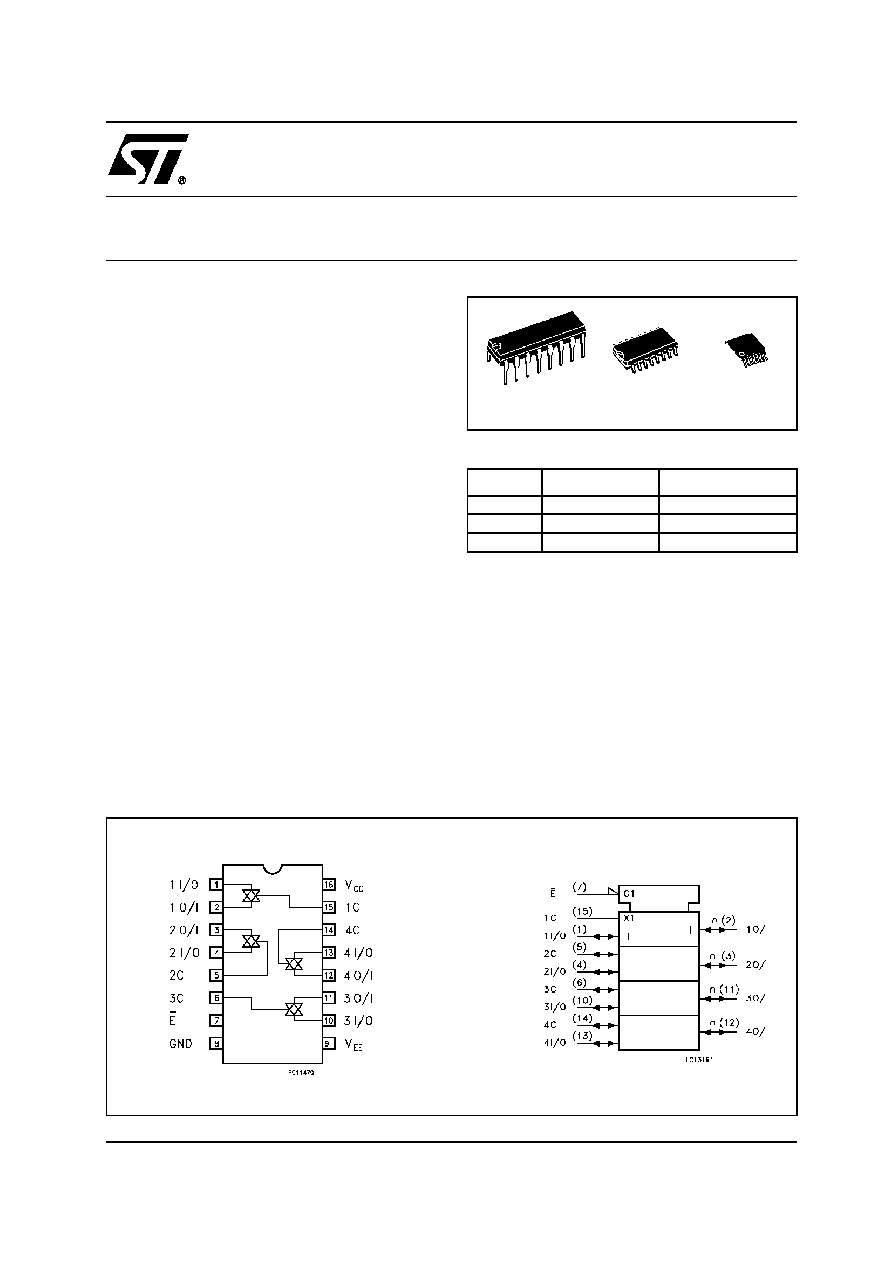
PIN CONNECTION AND IEC LOGIC SYMBOLS
ORDER CODES
PACKAGE
TUBE
T & R
DIP
M74HC4316B1R
SOP
M74HC4316M1R
M74HC4316RM13TR
TSSOP
M74HC4316TTR
TSSOP
DIP
SOP
QUAD BILATERAL SWITCH

M74HC4316
2/11
LOGIC DIAGRAM
PIN DESCRIPTION
TRUTH TABLE
ABSOLUTE MAXIMUM RATINGS
Absolute Maximum Ratings are those values beyond which damage to the device may occur. Functional operation under these conditions is
not implied
(*) 500mW at 65
∞
C; derate to 300mW by 10mW/
∞
C from 65
∞
C to 85
∞
C
PIN No
SYMBOL
NAME AND FUNCTION
1, 4, 10, 13
1 to 4 I/O
Independent Inputs/Out-
puts
2, 3, 11, 12
1 to 4 O/I
Independent Outputs/
Inputs
7
E
Enable Inputs (Active
LOW)
15, 5, 6, 14
1C to 4C
Enable Inputs (Active
High)
9
V
EE
Negative Supply Voltage
8
GND
Ground (0V)
16
V
CC
Positive Supply Voltage
E
C
SWITCH FUNCTION
L
H
ON
L
L
OFF
H
X
OFF
Symbol
Parameter
Value
Unit
V
CC
Supply Voltage
-0.5 to +7
V
V
CC
- V
EE
Supply Voltage
-0.5 to +13
V
V
I
Control Input Voltage
-0.5 to V
CC
+ 0.5
V
V
I/O
Switch Input/Out put Voltage
V
EE
-0.5 to V
CC
+ 0.5
V
I
IK
DC Input Diode Current
±
20
mA
I
OK
DC Output Diode Current
±
20
mA
I
O
DC Output Source Sink Current Per Output Pin
±
25
mA
I
CC
or I
GND
DC V
CC
or Ground Current
±
50
mA
P
D
Power Dissipation
500(*)
mW
T
stg
Storage Temperature
-65 to +150
∞
C
T
L
Lead Temperature (10 sec)
300
∞
C

M74HC4316
3/11
RECOMMENDED OPERATING CONDITIONS
DC SPECIFICATIONS
Symbol
Parameter
Value
Unit
V
CC
Supply Voltage
2 to 12
V
V
EE
Supply Voltage
-6 to 0
V
V
CC
- V
EE
Supply Voltage
2 to 12
V
V
I
Input Voltage
0 to V
CC
V
V
I/O
Switch I/O Voltage
0 to V
CC
V
T
op
Operating Temperature
-55 to 125
∞
C
t
r
, t
f
Input Rise and Fall Time
V
CC
= 2.0V
0 to 1000
ns
V
CC
= 4.5V
0 to 500
V
CC
= 6.0V
0 to 400
Symbol
Parameter
Test Conditio n
Value
Unit
V
CC
(V)
V
EE
(V)
T
A
= 25
∞
C
-40 to 85
∞
C
-55 to 125
∞
C
Min.
Typ.
Max.
Min.
Max.
Min.
Max.
V
IHC
High Level
Control Input
Voltage
2.0
1.5
1.5
1.5
V
4.5
3.15
3.15
3.15
6.0
4.2
4.2
4.2
V
ILC
Low Level Control
Input Voltage
2.0
0.5
0.5
0.5
V
4.5
1.35
1.35
1.35
6.0
1.8
1.8
1.8
R
ON
ON Resistance
4.5
GND
V
I
= V
IHC
V
I/O
= V
CC
to V
EE
I
I/O
=
0.1mA
70
170
200
4.5
-4.5
50
85
105
6.0
-6.0
30
70
85
2.0
GND
V
I
= V
IHC
V
I/O
= V
CC
or V
EE
I
I/O
=
0.1mA
120
180
215
4.5
GND
50
80
100
4.5
-4.5
35
60
75
6.0
-6.0
20
40
60
R
ON
Difference of ON
Resistance
between switches
4.5
GND V
IN
= V
IHC
or V
ILC
V
I/O
= V
CC
to V
EE
I
I/O
=
0.1mA
10
15
20
4.5
-4.5
5
10
15
6.0
-6.0
5
10
15
I
OFF
Input/Output
Leakage Current
(SWIT CH OFF)
6.0
GND V
OS
= V
CC
or GND
V
IS
= V
CC
or GND
V
IN
= V
IHC
or V
ILC
±
0.06
±
0.6
±
2
µ
A
6.0
-6.0
±
0.1
±
1
±
2
I
IZ
Switch Input
Leakage Current
(SWIT CH ON,
OUTPUT OPEN)
6.0
GND
V
OS
= V
CC
or GND
V
IN
= V
IHC
or V
ILC
±
0.06
±
0.6
±
2
µ
A
6.0
-6.0
±
0.1
±
1
±
2
I
IN
Control Input
Current
6.0
V
I
= V
CC
or GND
10
-5
±
0.1
±
1
±
1
µ
A

M74HC4316
4/11
AC ELECTRICAL CHARACTERISTICS (C
L
= 50 pF, Input t
r
= t
f
= 6ns)
CAPACITIVE CHARACTERISTICS
1) C
PD
is defined as the value of the IC's internal equivalent capacitance which is calculated from the operating current consumption without
load. (Refer to Test Circuit). Average operating current can be obtained by the following equation. I
CC(opr)
= C
PD
x V
CC
x f
IN
+ I
CC
Symbol
Parameter
Test Condition
Value
Unit
V
CC
(V)
V
EE
(V)
T
A
= 25
∞
C
-40 to 85
∞
C
-55 to 125
∞
C
Min.
Typ.
Max.
Min.
Max.
Min.
Max.
I/O
Phase Difference
Between Input
and Output
2.0
GND
12
30
40
ns
4.5
GND
3
6
8
6.0
GND
3
5
7
4.5
-4.5
2
4
5
6.0
-6.0
2
4
5
t
PZL
t
PZH
Output Enable
Time
(E, C - OUT)
2.0
GND
R
L
= 1K
56
115
145
ns
4.5
GND
14
23
29
6.0
GND
12
20
25
4.5
-4.5
13
21
26
6.0
-6.0
11
18
23
t
PLZ
t
PHZ
Output Disable
Time
(E, C - OUT)
2.0
GND
R
L
= 1K
112
205
255
ns
4.5
GND
28
41
51
6.0
GND
24
35
43
4.5
-4.5
24
34
43
6.0
-6.0
21
29
36
f
MAX
Maximum Control
Input Frequency
2.0
GND
R
L
= 1K
C
L
= 15 pF
V
OUT
= 1/2 V
CC
2
MHz
4.5
GND
9
6.0
GND
11
Symbol
Parameter
Test Condition
Value
Unit
V
CC
(V)
T
A
= 25
∞
C
-40 to 85
∞
C
-55 to 125
∞
C
Min.
Typ.
Max.
Min.
Max.
Min.
Max.
C
IN
Input Capacitance
5
10
10
10
pF
C
I/O
Switch Terminal
Capacitance
4.5
-4.5
5
pF
C
IOS
Feed Through
Capacitance
4.5
-4.5
1
pF
C
PD
Power Dissipation
Capacitance
(note 1)
5.0
GND
16
pF

M74HC4316
5/11
ANALOG SWITCH CHARACTERISTICS (GND = 0V;T
A
= 25
∞
C)
Symbol
Parameter
Test Condition
Value Unit
V
CC
(V)
V
EE
(V)
V
IN
(V
p-p
)
Typ.
Sine Wave
Distortion (THD)
2.25
2.25
4
f
IN
= 1 KHz R
L
= 10 K
, C
L
= 50 pF
0.025
%
4.5
4.5
8
0.020
6.0
6.0
11
0.018
f
MAX
Frequency
Response
(Switch ON)
2.25
2.25
Adjust f
IN
voltage to obtain 0 dBm at V
OS
.
Increase f
IN
Frequency until dB meter reads -3dB
R
L
= 50
, C
L
= 10 pF, f
IN
= 1MHz sine wave
28
MHz
4.5
4.5
42
6.0
6.0
43
Feed through
Attenuation
(Switch OFF )
2.25
2.25
V
IN
is centered at V
CC
/2. Adjust input for 0 dBm
R
L
= 600
, C
L
= 50 pF, f
IN
= 1MHz sine wave
-50
dB
4.5
4.5
-50
6.0
6.0
-50
Crosstalk (Control
Input to Signal
Output)
2.25
2.25
R
L
= 600
, C
L
= 50 pF, f
IN
= 1MHz square wave (t
r
= t
f
=6ns)
mV
4.5
4.5
5
6.0
6.0
Crosstalk
(Between Any
Switches)
2.25
2.25
Adjust V
IN
to Obtain 0 dBm at input
R
L
= 600
, C
L
= 50 pF, f
IN
= 1MHz sine wave
-50
dB
4.5
4.5
-50
6.0
6.0
-50

M74HC4316
6/11
SWITCHING CARACTERISTICS TEST CIRCUIT
CONTROL
BANDWIDTH AND FEEDTHROUGH ATTENUATION
MAXIMUM CONTROL FREQUENCY
ENABLE
CROSSTALK BETWEEN ANY TWO SWIT CHES
CROSSTALK (control to output)

M74HC4316
7/11
CHANNEL RESISTANCE (R
ON)
I
CC
(Opr.)

M74HC4316
8/11
DIM.
mm.
inch
MIN.
TYP
MAX.
MIN.
TYP.
MAX.
a1
0.51
0.020
B
0.77
1.65
0.030
0.065
b
0.5
0.020
b1
0.25
0.010
D
20
0.787
E
8.5
0.335
e
2.54
0.100
e3
17.78
0.700
F
7.1
0.280
I
5.1
0.201
L
3.3
0.130
Z
1.27
0.050
Plastic DIP-16 (0.25) MECHANICAL DATA
P001C

M74HC4316
9/11
DIM.
mm.
inch
MIN.
TYP
MAX.
MIN.
TYP.
MAX.
A
1.75
0.068
a1
0.1
0.2
0.003
0.007
a2
1.65
0.064
b
0.35
0.46
0.013
0.018
b1
0.19
0.25
0.007
0.010
C
0.5
0.019
c1
45
∞
(typ.)
D
9.8
10
0.385
0.393
E
5.8
6.2
0.228
0.244
e
1.27
0.050
e3
8.89
0.350
F
3.8
4.0
0.149
0.157
G
4.6
5.3
0.181
0.208
L
0.5
1.27
0.019
0.050
M
0.62
0.024
S
8
∞
(max.)
SO-16 MECHANICAL DATA
PO13H

M74HC4316
10/11
DIM.
mm.
inch
MIN.
TYP
MAX.
MIN.
TYP.
MAX.
A
1.2
0.047
A1
0.05
0.15
0.002
0.004
0.006
A2
0.8
1
1.05
0.031
0.039
0.041
b
0.19
0.30
0.007
0.012
c
0.09
0.20
0.004
0.0089
D
4.9
5
5.1
0.193
0.197
0.201
E
6.2
6.4
6.6
0.244
0.252
0.260
E1
4.3
4.4
4.48
0.169
0.173
0.176
e
0.65 BSC
0.0256 BSC
K
0
∞
8
∞
0
∞
8
∞
L
0.45
0.60
0.75
0.018
0.024
0.030
TSSOP16 MECHANICAL DATA
c
E
b
A2
A
E1
D
1
PIN 1 IDENTIFICATION
A1
L
K
e
0080338D

M74HC4316
Information furnished is believed to be accurate and reliable. However, STMicroelectronics assumes no responsibility for the
consequences of use of such inform ation nor for any infringe ment of patents or other righ ts of third parties which may result from
its use. No license is granted by implication or otherwise under any patent or patent rights of STMicroelectronics. Specifications
mentioned in this pub lication are subject to change without notice. Thi s pub lication supersedes and replaces all information
previously supplied. STMicroelectronics prod ucts are not authori zed for use as critical components in life suppo rt devices or
systems without express written approval of STMicroelectronics.
©
The ST logo is a registered trademark of STMicroelectronics
©
2001 STMicroelectronics - Printed in Italy - All Rights Reserved
STMicroelectronics GROUP OF COMPANIES
Australia - Brazil - China - Finland - France - Germany - Hong Kong - India - Italy - Japan - Malaysia - Malta - Morocco
Singapore - Spain - Sweden - Swit zerland - United Kingdom
©
http://w ww.st.com
11/11