
M74HC646
M74HC648
October 1993
HC648 OCTAL BUS TRANSCEIVER/REGISTER (3-STATE, INV.)
HC646 OCTAL BUS TRANSCEIVER/REGISTER (3-STATE)
B1R
(Plastic Package)
ORDER CODES :
M74HCXXXM1R
M74HCXXXB1R
M1R
(Micro Package)
INPUT AND OUTPUT EQUIVALENT CIRCUIT
PIN CONNECTIONS (top view)
GAB, GAB, CAB,
A, B
SAB, SBA, CBA
.
HIGH SPEED
f
MAX
= 73 MHz (TYP.) AT V
CC
= 5 V
.
LOW POWER DISSIPATION
I
CC
= 4
µ
A (MAX.) AT T
A
= 25
∞
C
.
HIGH NOISE IMMUNITY
V
NIH
= V
NIL
= 28 % V
CC
(MIN.)
.
OUTPUT DRIVE CAPABILITY
15 LSTTL LOADS
.
SYMMETRICAL OUTPUT IMPEDANCE
I
OH
= I
OL
= 6 mA (MIN.)
.
BALANCED PROPAGATION DELAYS
t
PLH
= t
PHL
.
WIDE OPERATING VOLTAGE RANGE
V
CC
(OPR) = 2 V TO 6 V
.
PIN AND FUNCTION COMPATIBLE
WITH 54/74LS646/648
DESCRIPTION
The M74HC646/648 are high speed CMOS OCTAL
BUS TRANSCEIVERS AND REGISTERS, (3-
STATE) fabricated in silicon gate C
2
MOS technol-
ogy. They have the same high speed performance
of LSTTL combined with true CMOS low power con-
sumption.
These devices consist of bus transceiver circuits
with 3-state output, D-type flip-flops, and control cir-
cuitry arranged for multiplexed transmission of data
directly from the input bus or from the internal reg-
isters. Data on the A or B bus will be clocked into the
registers on the low-to-high transition of the appro-
priate clock pin (Clock AB - or Clock BA). Enable (G)
and direction (DIR) pins are provided to control the
transceiver functions. In the transceiver mode, data
present at the high-impedance port may be stored
in either register or in both.
The select controls (Select AB select BA) can multi-
plex stored and real-time (transparent mode) data.
The direction control determines which bus will re-
ceive data when enable G is active (low).
In the isolation mode (enable G high), "A" data may
be stored in one register and/or "B" data may be
stored in the other register. When an output function
is disabled, the input function is still enabled and
may be used to store and transmit data. Only one
of the two buses, A or B, may be driven at a time.
All inputs are equipped with protection circuits
1/12
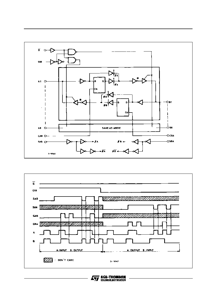
LOGIC DIAGRAM (HC648)
Note : In case of M54/74HC646 output inverter marked * at A bus and B bus are eliminated.
TIMING CHART
M74HC646/648
2/12

TRUTH TABLE
HC646 (The truth table for HC648 is the same as this, but with the outputs inverted)
G
DIR
CAB CBA SAB SBA
A
B
FUNCTION
H
X
INPUTS
INPUTS
Both the A bus and the B bus are inputs
X
X
X
X
Z
Z
The output functions of the A and B bus are disabled
X
X
INPUTS
INPUTS
Both the A and B bus are used for inputs to the
internal flip-flops. Data at the bus will be stored on
low to high transition of the clock inputs
L
H
INPUTS
OUTPUTS
The A bus are inputs and the B bus are outputs
X
X*
L
X
L
L
The data at the A bus are displayed at the B bus
H
H
X*
L
X
L
L
The data at the A bus are displayed at the B bus.
The data of the A bus are stored to the internal
flip-flop on low to high transition of th clock pulse.
H
H
X
X*
H
X
X
Qn
The data stored to the internal flip-flop are dispayed
at the B bus
X*
H
X
L
L
The data at the A bus are stored to the internal flip-
flop on low to high transition of the clock pulse. The
states of the internal flip-flops output directly to the
B bus
H
H
L
L
OUTPUTS
INPUTS
The B bus are inputs and the A bus are outputs
X*
X
X
L
L
L
The data at the B bus are displayed at the A bus
H
H
X*
X
L
L
L
The data at the B bus are displayed at the A bus.
The data of the B bus are stored to the internal flip-
flop on low to high transition of the clock pulse
H
H
X*
X
X
H
Qn
X
The data stored to the internal flip-flops are
displayed at the A bus
x*
X
H
L
L
the data at the B bus are stored to the internal flip-
flop on low to high transition of the clock pulse. The
states of the internal flip-flops output directly to the
A bus
H
H
X
: DON'T CARE
Z
: HIGH IMPEDANCE
Qn
: THE DATA STORED TO THE INTERNAL FLIP-FLOPS BY MOST RECENT LOW TO HIGH TRANSITION OF THE CLOCK INPUTS
*
: THE DATA AT THE A AND B BUS WILL BE STORED TO THE INTERNAL FLIP-FLOPS ON EVERY LOW TO HIGH TRANSITION OF
THE CLOCK INPUTS
M74HC646/648
3/12

PIN DESCRIPTION
PIN No
SYMBOL
NAME AND FUNCTION
1
CLOCK AB
A to B Clock Input (LOW to HIGH, Edge-Trigged)
2
SELECT AB
Select A to B Source Input
3
GAB
Direction Control Input
4, 5, 6, 7, 8, 9, 10, 11
A1 to A8
A data Inputs/Outputs
20, 19, 18, 17, 16, 15, 14, 13
B1 to B8
B Data Inputs/Outputs
21
G
Output Enable Input (Active LOW)
22
SELECT BA
Select B to A Source Input
23
CLOCK BA
B to A Clock Input (LOW to HIGH, Edge-Triggered)
12
GND
Ground (0V)
24
V
CC
Positive Supply Voltage
IEC LOGIC SYMBOLS
HC646
HC648
M74HC646/648
4/12

ABSOLUTE MAXIMUM RATINGS
Symbol
Parameter
Value
Unit
V
CC
Supply Voltage
-0.5 to +7
V
V
I
DC Input Voltage
-0.5 to V
CC
+ 0.5
V
V
O
DC Output Voltage
-0.5 to V
CC
+ 0.5
V
I
IK
DC Input Diode Current
±
20
mA
I
OK
DC Output Diode Current
±
20
mA
I
O
DC Output Source Sink Current Per Output Pin
±
35
mA
I
CC
or I
GND
DC V
CC
or Ground Current
±
70
mA
P
D
Power Dissipation
500 (*)
mW
T
stg
Storage Temperature
-65 to +150
o
C
T
L
Lead Temperature (10 sec)
300
o
C
Absolute Maximum Ratings are those values beyond which damage to the device may occur. Functional operation under these condition is not implied.
(*) 500 mW:
65
o
C derate to 300 mW by 10mW/
o
C: 65
o
C to 85
o
C
RECOMMENDED OPERATING CONDITIONS
Symbol
Parameter
Value
Unit
V
CC
Supply Voltage
2 to 6
V
V
I
Input Voltage
0 to V
CC
V
V
O
Output Voltage
0 to V
CC
V
T
op
Operating Temperature
-40 to +85
o
C
t
r
, t
f
Input Rise and Fall Time
V
CC
= 2 V
0 to 1000
ns
V
CC
= 4.5 V
0 to 500
V
CC
= 6 V
0 to 400
M74HC646/648
5/12
DC SPECIFICATIONS
Symbol
Parameter
Test Conditions
Value
Unit
V
CC
(V)
T
A
= 25
o
C
-40 to 85
o
C
Min.
Typ.
Max.
Min.
Max.
V
IH
High Level Input Voltage
2.0
1.5
1.5
V
4.5
3.15
3.15
6.0
4.2
4.2
V
IL
Low Level Input
Voltage
2.0
0.5
0.5
V
4.5
1.35
1.35
6.0
1.8
1.8
V
OH
High Level Output Voltage
2.0
V
I
=
V
IH
or
V
IL
I
O
=-20
µ
A
1.9
2.0
1.9
V
4.5
4.4
4.5
4.4
6.0
5.9
6.0
5.9
4.5
I
O
=-6.0 mA
4.18
4.31
4.13
6.0
I
O
=-7.8 mA
5.68
5.8
5.63
V
OL
Low Level Output Voltage
2.0
V
I
=
V
IH
or
V
IL
I
O
= 20
µ
A
0.0
0.1
0.1
V
4.5
0.0
0.1
0.1
6.0
0.0
0.1
0.1
4.5
I
O
= 6.0 mA
0.17
0.26
0.37
6.0
I
O
= 7.8 mA
0.18
0.26
0.37
I
I
Input Leakage Current
6.0
V
I
= V
CC
or GND
±
0.1
±
1
µ
A
I
OZ
3 State Output Off State Current
6.0
V
I
= V
IH
or V
IL
V
O
= V
CC
or GND
±
0.5
±
5.0
µ
A
I
CC
Quiescent Supply Current
6.0
V
I
= V
CC
or GND
4
40
µ
A
AC ELECTRICAL CHARACTERISTICS (C
L
= 50 pF, Input t
r
= t
f
= 6 ns)
Symbol
Parameter
Test Conditions
Value
Unit
V
CC
(V)
C
L
(pF)
T
A
= 25
o
C
-40 to 85
o
C
Min.
Typ.
Max.
Min.
Max.
t
TLH
t
THL
Output Transition Time
2.0
50
25
60
75
ns
4.5
7
12
15
6.0
6
10
13
t
PLH
t
PHL
Propagation Delay Time
(BUS - BUS)
2.0
50
74
150
190
ns
4.5
21
30
38
6.0
18
26
32
2.0
150
91
190
240
ns
4.5
26
38
48
6.0
22
32
41
t
PLH
t
PHL
Propagation Delay Time
(CLOCK - BUS)
2.0
50
98
210
265
ns
4.5
28
42
53
6.0
24
36
45
2.0
150
116
250
315
ns
4.5
33
50
63
6.0
28
43
54
M74HC646/648
6/12

AC ELECTRICAL CHARACTERISTICS (C
L
= 50 pF, Input t
r
= t
f
= 6 ns)
Symbol
Parameter
Test Conditions
Value
Unit
V
CC
(V)
C
L
(pF)
T
A
= 25
o
C
-40 to 85
o
C
Min.
Typ.
Max.
Min.
Max.
t
PLH
t
PHL
Propagation Delay Time
(SELECT - BUS)
2.0
50
81
170
215
ns
4.5
23
34
43
6.0
20
29
37
2.0
150
98
210
265
ns
4.5
28
42
53
6.0
24
36
45
t
PZL
t
PZH
3-State Output Enable Time
(G, DIR)
2.0
50
R
L
= 1 K
84
175
220
ns
4.5
24
35
44
6.0
20
30
37
2.0
150
R
L
= 1 K
102
215
270
ns
4.5
29
43
54
6.0
25
37
46
t
PLZ
t
PHZ
Output Disable Time
(G, DIR)
2.0
50
R
L
= 1 K
60
175
220
ns
4.5
23
35
44
6.0
20
30
37
f
MAX
Maximum Clock Frequency
2.0
50
6
19
4.8
MHz
4.5
30
67
24
6.0
35
79
28
t
W(H)
t
W(L)
Minimum Clock Pulse Width
2.0
50
30
75
95
ns
4.5
7
15
19
6.0
6
13
16
t
s
Minimum Set-up Time
2.0
50
16
50
65
ns
4.5
4
10
13
6.0
3
9
11
t
h
Minimum Hold Time
2.0
50
5
5
ns
4.5
5
5
6.0
5
5
C
IN
Input Capacitance
5
10
10
pF
C
I/O
Bus Terminal Capacitance
10
pF
C
PD
(*)
Power Dissipation Capacitance
for HC646
for HC648
39
38
pF
(*) C
PD
is defined as the value of the IC's internal equivalent capacitance which is calculated from the operating current consumption without load.
(Refer to Test Circuit). Average operting current can be obtained by the following equation. I
CC
(opr) = C
PD
∑
V
CC
∑
f
IN
+ I
CC
/8 (per bit)
M74HC646/648
7/12

SWITCHING CHARACTERISTICS TEST CIRCUIT AND WAVEFORM
WAVEFORM 1
WAVEFORM 2
WAVEFORM 3
WAVEFORM 4
WAVEFORM 5
M74HC646/648
8/12

* INPUT TRANSITION TIME IS THE SAME AS THAT IN CASE OF SWITCHING CHARACTERISTICS TEST.
TEST WAVEFORM I
CC
(Opr.)
M74HC646/648
9/12

Plastic DIP24 (0.25) MECHANICAL DATA
DIM.
mm
inch
MIN.
TYP.
MAX.
MIN.
TYP.
MAX.
a1
0.63
0.025
b
0.45
0.018
b1
0.23
0.31
0.009
0.012
b2
1.27
0.050
D
32.2
1.268
E
15.2
16.68
0.598
0.657
e
2.54
0.100
e3
27.94
1.100
F
14.1
0.555
I
4.445
0.175
L
3.3
0.130
P043A
M74HC646/648
10/12

SO24 MECHANICAL DATA
DIM.
mm
inch
MIN.
TYP.
MAX.
MIN.
TYP.
MAX.
A
2.65
0.104
a1
0.10
0.20
0.004
0.007
a2
2.45
0.096
b
0.35
0.49
0.013
0.019
b1
0.23
0.32
0.009
0.012
C
0.50
0.020
c1
45
∞
(typ.)
D
15.20
15.60
0.598
0.614
E
10.00
10.65
0.393
0.420
e
1.27
0.05
e3
13.97
0.55
F
7.40
7.60
0.291
0.299
L
0.50
1.27
0.19
0.050
S
8
∞
(max.)
F
C
L
E
a1
b1
A
e
D
e3
b
24
13
1
12
c1
s
a2
M74HC646/648
11/12

Information furnished is believed to be accurate and reliable. However, SGS-THOMSON Microelectronics assumes no responsability for the
consequences of use of such information nor for any infringement of patents or other rights of third parties which may results from its use. No
license is granted by implication or otherwise under any patent or patent rights of SGS-THOMSON Microelectronics. Specifications mentioned
in this publication are subject to change without notice. This publication supersedes and replaces all information previously supplied.
SGS-THOMSON Microelectronics products are not authorized for use as critical components in life support devices or systems without express
written approval of SGS-THOMSON Microelectonics.
©
1994 SGS-THOMSON Microelectronics - All Rights Reserved
SGS-THOMSON Microelectronics GROUP OF COMPANIES
Australia - Brazil - France - Germany - Hong Kong - Italy - Japan - Korea - Malaysia - Malta - Morocco - The Netherlands -
Singapore - Spain - Sweden - Switzerland - Taiwan - Thailand - United Kingdom - U.S.A
M74HC646/648
12/12