M54HCT14
M74HCT14
October 1993
HEX SCHMITT INVERTER
B1R
(Plastic Package)
ORDER CODES :
M54HCT14F1R
M74HCT14M1R
M74HCT14B1R
M74HCT14C1R
F1R
(Ceramic Package)
M1R
(Micro Package)
C1R
(Chip Carrier)
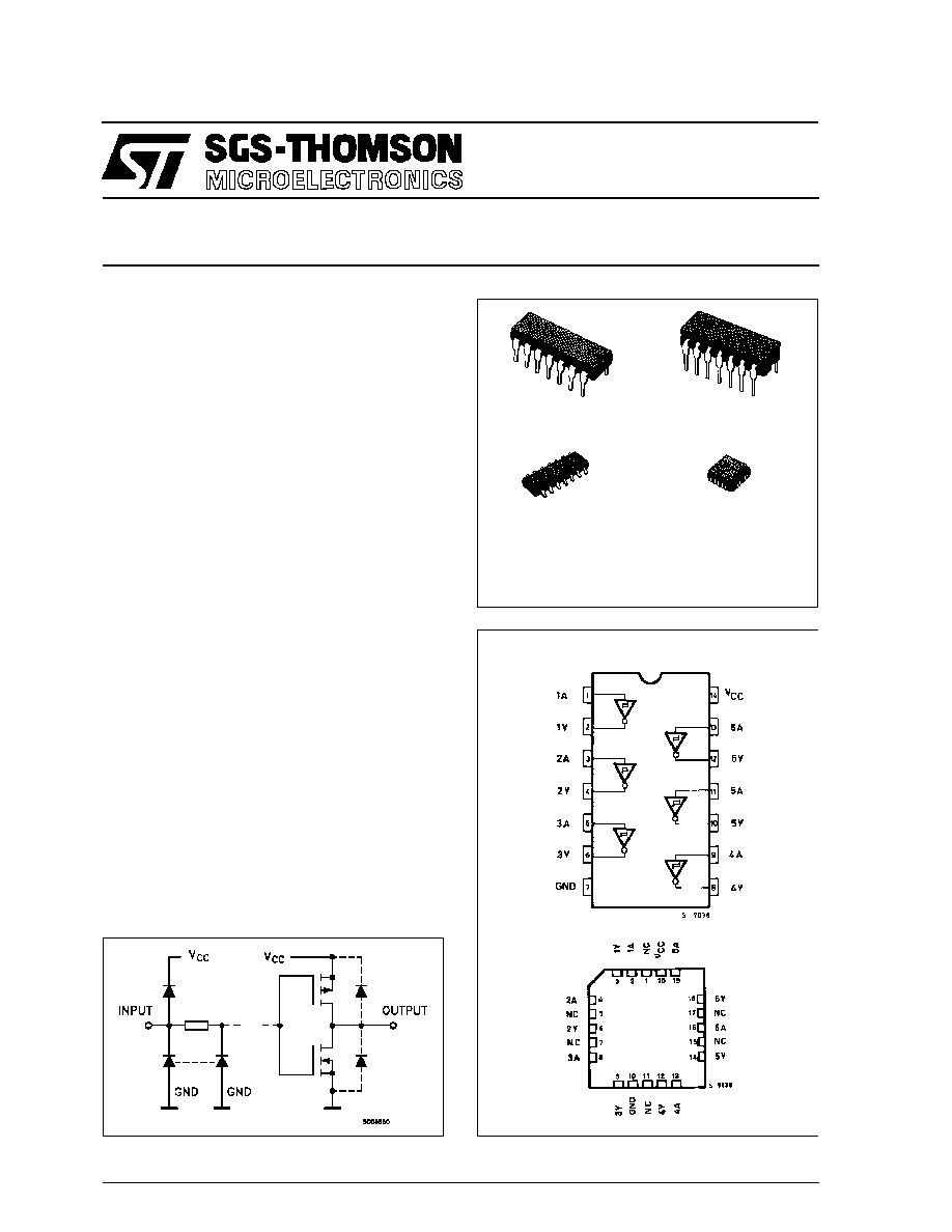
PIN CONNECTIONS (top view)
NC =
No Internal
Connection
INPUT AND OUTPUT EQUIVALENT CIRCUIT
.
HIGH SPEED
t
PD
= 16 ns (TYP.) AT V
CC
= 5 V
.
LOW POWER DISSIPATION
I
CC
= 1
�
A (MAX.) AT T
A
= 25
�
C
.
HIGH NOISE IMMUNITY
V
H
= 0.7 V (TYP.) AT V
CC
= 5 V
.
OUTPUT DRIVE CAPABILITY
10 LSTTL LOADS
.
SYMMETRICAL OUTPUT IMPEDANCE
IOH
= I
OL
= 4 mA (MIN.)
.
BALANCED PROPAGATION DELAYS
t
PLH
= t
PHL
.
PIN AND FUNCTION COMPATIBLE WITH
54/74LS14
The M54/74HCT14 is a high speed CMOS HEX
SCHMITT INVERTER fabricated in silicon gate
C
2
MOS technology. It has the same high speed per-
formance of LSTTL combined with true CMOS low
power consumption. Pin configuration and function
are the same as those of the HCT04 but all inputs
have 0.7 V hysteresis level.This together with its
schmitt trigger function allows it to be used on line
receivers with slow rise/fall input signals. This inte-
grated circuit has input and output characteristics
that are fully compatible with 54/74 LSTTL logic
families. M54/74HCT devices are designed to di-
rectly interface HSC
2
MOS systems with TTL and
NMOS components. They are also plug in replace-
ments for LSTTL devices giving a reduction of
power consumption.All inputs are equipped with pro-
DESCRIPTION
1/9
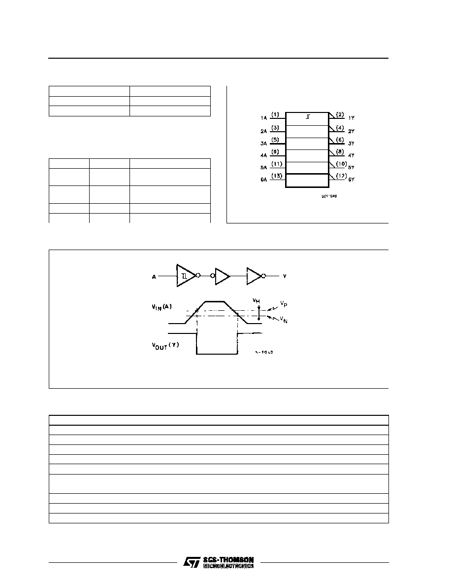
TRUTH TABLE
A
Y
L
H
H
L
PIN DESCRIPTION
PIN No
SYMBOL
NAME AND FUNCTION
1, 3, 5, 9,
11, 13
1A to 6A
Data Inputs
2, 4, 6, 8,
10,12
1Y to 6Y
Data Outputs
7
GND
Ground (0V)
14
V
CC
Positive Supply Voltage
IEC LOGIC SYMBOL
LOGIC DIAGRAM/WAVEFORM
ABSOLUTE MAXIMUM RATINGS
Symbol
Parameter
Value
Unit
V
CC
Supply Voltage
-0.5 to +7
V
V
I
DC Input Voltage
-0.5 to V
CC
+ 0.5
V
V
O
DC Output Voltage
-0.5 to V
CC
+ 0.5
V
I
IK
DC Input Diode Current
�
20
mA
I
OK
DC Output Diode Current
�
20
mA
I
O
DC Output Source Sink Current Per Output Pin
�
25
mA
I
CC
or I
GND
DC V
CC
or Ground Current
�
50
mA
P
D
Power Dissipation
500 (*)
mW
T
stg
Storage Temperature
-65 to +150
o
C
T
L
Lead Temperature (10 sec)
300
o
C
Absolute Maximum Ratings are those values beyond which damage to the device may occur. Functional operation under these condition is not implied.
(*) 500 mW:
65
o
C derate to 300 mW by 10mW/
o
C: 65
o
C to 85
o
C
M54/M74HCT14
2/9
RECOMMENDED OPERATING CONDITIONS
Symbol
Parameter
Value
Unit
V
CC
Supply Voltage
4.5 to 5.5
V
V
I
Input Voltage
0 to V
CC
V
V
O
Output Voltage
0 to V
CC
V
T
op
Operating Temperature: M54HC Series
M74HC Series
-55 to +125
-40 to +85
o
C
o
C
DC SPECIFICATIONS
Symbol
Parameter
Test Conditions
Value
Unit
V
CC
(V)
T
A
= 25
o
C
54HC and 74HC
-40 to 85
o
C
74HC
-55 to 125
o
C
54HC
Min.
Typ.
Max.
Min.
Max.
Min.
Max.
V
P
High Level
Threshold Voltage
4.5
1.2
1.55
1.9
1.2
1.9
1.2
1.9
V
5.5
1.4
1.75
2.1
1.4
2.1
1.4
2.1
V
N
High Level
Threshold Voltage
4.5
0.5
0.85
1.2
0.5
1.2
0.5
1.2
V
5.5
0.6
1.1
1.4
0.6
1.4
0.6
1.4
V
H
Hysteresis
Voltage
4.5
0.4
0.7
1.4
0.4
1.4
0.4
1.4
V
5.5
0.4
0.7
1.5
0.4
1.5
0.4
1.5
V
OH
High Level
Output Voltage
4.5
V
I
=
V
IH
or
V
IL
I
O
=-20
�
A
4.4
4.5
4.4
4.4
V
I
O
=-4.0 mA
4.18
4.31
4.13
4.10
V
OL
Low Level Output
Voltage
4.5
V
I
=
V
IH
or
V
IL
I
O
= 20
�
A
0.0
0.1
0.1
0.1
V
I
O
= 4.0 mA
0.17
0.26
0.33
0.4
I
I
Input Leakage
Current
5.5
V
I
= V
CC
or GND
�
0.1
�
1
�
1
�
A
I
CC
Quiescent Supply
Current
5.5
V
I
= V
CC
or GND
1
10
20
�
A
M54/M74HCT14
3/9

SWITCHING CHARACTERISTICS TEST CIRCUIT
INPUT WAVEFORM IS THE SAME AS THAT IN CASE OF SWITCHING CHARACTERISTICS TEST.
TEST CIRCUIT I
CC
(Opr.)
AC ELECTRICAL CHARACTERISTICS (C
L
= 50 pF, Input t
r
= t
f
= 6 ns)
Symbol
Parameter
Test Conditions
Value
Unit
V
CC
(V)
T
A
= 25
o
C
54HC and 74HC
-40 to 85
o
C
74HC
-55 to 125
o
C
54HC
Min.
Typ.
Max.
Min.
Max.
Min.
Max.
t
TLH
t
THL
Output Transition
Time
4.5
8
15
19
22
ns
t
PLH
t
PHL
Propagation
Delay Time
4.5
19
30
38
45
ns
C
IN
Input Capacitance
5
10
10
10
pF
C
PD
(*)
Power Dissipation
Capacitance
45
pF
(*) C
PD
is defined as the value of the IC's internal equivalent capacitance which is calculated from the operating current consumption without load.
(Refer to Test Circuit). Average operting current can be obtained by the following equation. I
CC
(opr) = C
PD
�
V
CC
�
f
IN
+ I
CC
M54/M74HCT14
4/9