
M54HCT164
M74HCT164
February 1993
8 BIT SIPO SHIFT REGISTER
B1R
(Plastic Package)
ORDER CODES :
M54HCT164F1R
M74HCT164M1R
M74HCT164B1R
M74HCT164C1R
F1R
(Ceramic Package)
M1R
(Micro Package)
C1R
(Chip Carrier)
PIN CONNECTIONS (top view)
NC =
No Internal
Connection
.
HIGH SPEED
t
PD
= 20 ns (TYP.) AT V
CC
= 5 V
.
LOW POWER DISSIPATION
I
CC
= 4
µ
A (MAX.) AT T
A
= 25
∞
C
.
OUTPUT DRIVE CAPABILITY
10 LSTTL LOADS
.
BALANCED PROPAGATION DELAYS
t
PLH
= t
PHL
= 4 mA (MIN.)
.
SYMMETRICAL OUTPUT IMPEDANCE
I
OL
=
I
OH
= 4 mA (MIN)
.
COMPATIBLE WITH TTL OUTPUTS
V
IH
= 2V (MIN.) V
IL
= 0.8V (MAX)
.
WIDE OPERATING VOLTAGE RANGE
V
CC
(OPR) = 2 V TO 6 V
.
PIN AND FUNCTION COMPATIBLE
WITH 54/74LS164
DESCRIPTION
The M54/74HCT164 is a high speed CMOS 8 BIT
SIPO SHIFT REGISTER fabricated in silicon gate
C
2
MOS technology. It has the same high speed per-
formance of LSTTL combined with true CMOS low
power consumption.
The HCT164 is an 8 bit shift register with serial data
entry and an output from each of the eight stages.
Data is entered serially through one of two inputs (A
or B), either of these inputs can be used as an active
high enable for data entry through the other input.
An unused input must be high, or both inputs con-
nected together. Each low-to-high transition on the
clock input shifts data one place to the right and
enters into QA, the logic NAND of the two data inputs
(A
∑
B), the data that existed before the rising clock
edge. A low level on the clear input overrides all
other inputs and clears the register asynchronously,
forcing all Q outputs low.
All inputs are equipped with protection circuits
against static discharge and transient excess volt-
age.
This integrated circuit has input and output charac-
teristics that are fully compatible with 54/74 LSTTL
logic families. M54/74HCT devices are designed to
directly interface HSC
2
MOS systems with TTL and
NMOS components. They are also plug in replace-
ments for LSTTL devices giving a reduction of
power consumption.
1/12
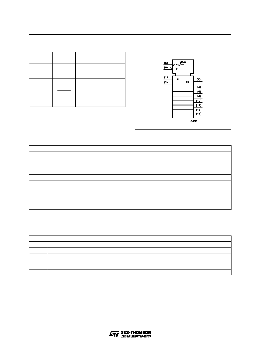
PIN DESCRIPTION
PIN No
SYMBOL
NAME AND FUNCTION
1, 2
A, B
Data Inputs
3, 4, 5, 6,
10, 11, 12,
13
QA to QH
Outputs
8
CLOCK
Clock Input (LOW to
HIGH, Edge-triggered)
9
CLEAR
Master Reset Input
7
GND
Ground (0V)
14
V
CC
Positive Supply Voltage
IEC LOGIC SYMBOL
ABSOLUTE MAXIMUM RATINGS
Symbol
Parameter
Value
Unit
V
CC
Supply Voltage
-0.5 to +7
V
V
I
DC Input Voltage
-0.5 to V
CC
+ 0.5
V
V
O
DC Output Voltage
-0.5 to V
CC
+ 0.5
V
I
IK
DC Input Diode Current
±
20
mA
I
OK
DC Output Diode Current
±
20
mA
I
O
DC Output Source Sink Current Per Output Pin
±
25
mA
I
CC
or I
GND
DC V
CC
or Ground Current
±
50
mA
P
D
Power Dissipation
500 (*)
mW
T
stg
Storage Temperature
-65 to +150
o
C
T
L
Lead Temperature (10 sec)
300
o
C
Absolute Maximum Ratings are those values beyond which damage to the device may occur. Functional operation under these condition is not implied.
(*) 500 mW:
65
o
C derate to 300 mW by 10mW/
o
C: 65
o
C to 85
o
C
RECOMMENDED OPERATING CONDITIONS
Symbol
Parameter
Value
Unit
V
CC
Supply Voltage
4.5 to 5.5
V
V
I
Input Voltage
0 to V
CC
V
V
O
Output Voltage
0 to V
CC
V
T
op
Operating Temperature: M54HC Series
M74HC Series
-55 to +125
-40 to +85
o
C
o
C
t
r
, t
f
Input Rise and Fall Time (V
CC
= 4.5 to 5.5V)
0 to 500
ns
M54/M74HCT164
3/12

AC ELECTRICAL CHARACTERISTICS (C
L
= 50 pF, Input t
r
= t
f
= 6 ns)
Symbol
Parameter
Test Conditions
Value
Unit
V
CC
(V)
T
A
= 25
o
C
54HC and 74HC
-40 to 85
o
C
74HC
-55 to 125
o
C
54HC
Min.
Typ.
Max.
Min.
Max.
Min.
Max.
t
TLH
t
THL
Output Transition
Time
4.5
8
15
19
22
ns
t
PLH
t
PHL
Propagation
Delay Time
(CLOCK - Q)
4.5
23
36
45
54
ns
t
PHL
Propagation
Delay Time
(CLEAR - Q)
4.5
24
37
46
56
ns
f
MAX
Maximum Clock
Frequency
4.5
30
50
24
20
MHz
t
W(H)
t
W(L)
Minimum Pulse
Width
(CLOCK)
4.5
8
15
19
22
ns
t
W(L)
Minimum Pulse
Width
(CLEAR)
4.5
8
15
19
22
ns
t
s
Minimum Set-up
Time
(A, B - CK)
4.5
4
10
13
15
ns
t
h
Minimum Hold
Time
(A, B - CK)
4.5
0
0
0
ns
t
REM
Minimum
Removal Time
5
6
8
ns
C
IN
Input Capacitance
5
10
10
10
pF
C
PD
(*)
Power Dissipation
Capacitance
137
pF
(*) C
PD
is defined as the value of the IC's internal equivalent capacitance which is calculated from the operating current consumption without load.
(Refer to Test Circuit). Average operting current can be obtained by the following equation. I
CC
(opr) = C
PD
∑
V
CC
∑
f
IN
+ I
CC
M54/M74HCT164
5/12

