
M54HCT273
M74HCT273
February 1993
OCTAL D TYPE FLIP FLOP WITH CLEAR
B1R
(Plastic Package)
ORDER CODES :
M54HCT273F1R
M74HCT273M1R
M74HCT273B1R
M74HCT273C1R
F1R
(Ceramic Package)
M1R
(Micro Package)
C1R
(Chip Carrier)
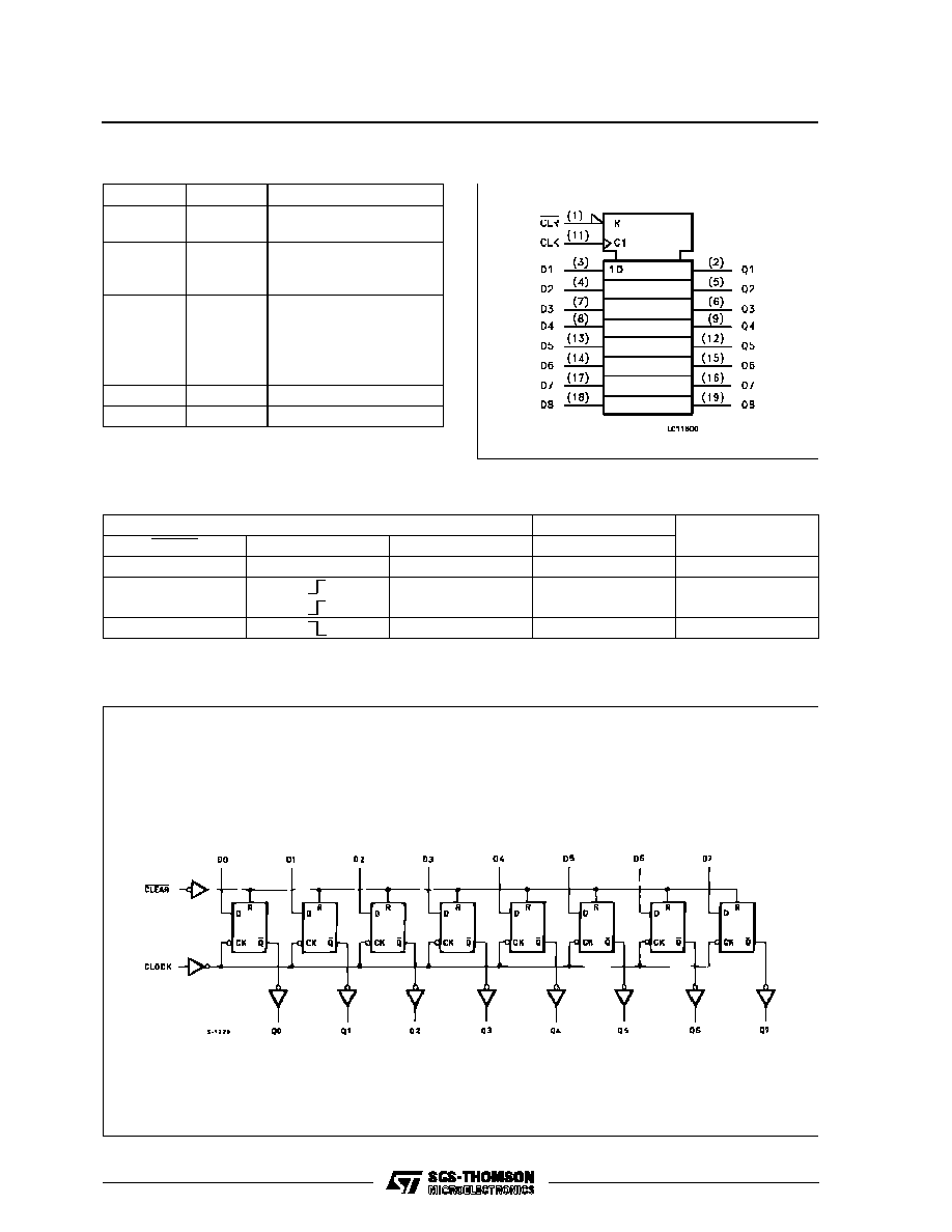
PIN CONNECTIONS (top view)
NC =
No Internal
Connection
.
HIGH SPEED
f
MAX
= 80 MHz (TYP.) AT V
CC
= 5 V
.
LOW POWER DISSIPATION
I
CC
= 4
µ
A (MAX.) AT T
A
= 25
∞
C
.
COMPATIBLE WITH TTL OUTPUTS
V
IH
= 2V (MIN.) V
IL
= 0.8V (MAX)
.
OUTPUT DRIVE CAPABILITY
10 LSTTL LOADS
.
SYMMETRICAL OUTPUT IMPEDANCE
IOH
= I
OL
= 4 mA (MIN.)
.
BALANCED PROPAGATION DELAYS
t
PLH
= t
PHL
.
PIN AND FUNCTION COMPATIBLE WITH
54/74LS273
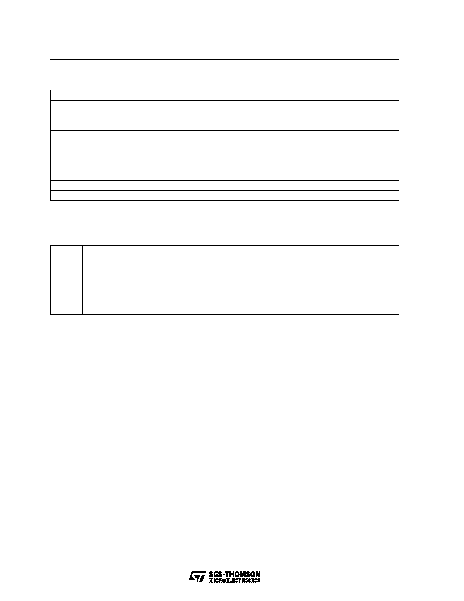
The M54/74HCT273 is a high speed CMOS OCTAL
D-TYPE FLIP FLOP WITH CLEAR fabricated in sili-
con gate C
2
MOS technology. It has the same high
speed performance of LSTTL combined with true
CMOS low power consumption. Information signals
applied to D inputs are transferred to the Q outputs
on the positive-going edge of the clock pulse.
When the CLEAR input is held low, the Q output are
in the low logic level independent of the other inputs.
All inputs are equipped with protection circuits
against static discharge and transient excess volt-
age. This integrated circuit has input and output
characteristics that are fully compatible with 54/74
LSTTL logic families. M54/74HCT devices are de-
signed to directly interface HSC
2
MOS systems with
TTL and NMOS components. They are also plug in
replacements for LSTTL devices giving a reduction
of power consumption. All inputs are equipped with
protection circuits against static discharge and tran-
sient excess voltage.
DESCRIPTION
INPUT AND OUTPUT EQUIVALENT CIRCUIT
1/10
TRUTH TABLE
INPUTS
OUTPUS
FUNCTION
CLEAR
CLOCK
D
QA
L
X
X
L
CLEAR
H
L
L
H
H
H
H
X
Qn
NO CHANGE
X: Don't Care
LOGIC DIAGRAM
PIN DESCRIPTION
PIN No
SYMBOL
NAME AND FUNCTION
1
CLEAR
Master Reset Input
(Active LOW)
2, 5, 6, 9,
12, 15, 16,
19
Q0 to Q7
Flip Flop Outputs
3, 4, 7, 8,
13, 14, 17,
18
D0 to D7
Data Inputs
11
CLOCK
Clock Input (LOW to
HIGH, Edge Triggered)
10
GND
Ground (0V)
20
V
CC
Positive Supply Voltage
IEC LOGIC SYMBOL
M54/M74HCT273
2/10
ABSOLUTE MAXIMUM RATINGS
Symbol
Parameter
Value
Unit
V
CC
Supply Voltage
-0.5 to +7
V
V
I
DC Input Voltage
-0.5 to V
CC
+ 0.5
V
V
O
DC Output Voltage
-0.5 to V
CC
+ 0.5
V
I
IK
DC Input Diode Current
±
20
mA
I
OK
DC Output Diode Current
±
20
mA
I
O
DC Output Source Sink Current Per Output Pin
±
25
mA
I
CC
or I
GND
DC V
CC
or Ground Current
±
50
mA
P
D
Power Dissipation
500 (*)
mW
T
stg
Storage Temperature
-65 to +150
o
C
T
L
Lead Temperature (10 sec)
300
o
C
Absolute Maximum Ratings are those values beyond which damage to the device may occur. Functional operation under these condition is not implied.
(*) 500 mW:
65
o
C derate to 300 mW by 10mW/
o
C: 65
o
C to 85
o
C
RECOMMENDED OPERATING CONDITIONS
Symbol
Parameter
Value
Unit
V
CC
Supply Voltage
4.5 to 5.5
V
V
I
Input Voltage
0 to V
CC
V
V
O
Output Voltage
0 to V
CC
V
T
op
Operating Temperature: M54HC Series
M74HC Series
-55 to +125
-40 to +85
o
C
o
C
t
r
, t
f
Input Rise and Fall Time (V
CC
= 4.5 to 5.5V)
0 to 500
ns
M54/M74HCT273
3/10

DC SPECIFICATIONS
Symbol
Parameter
Test Conditions
Value
Unit
V
CC
(V)
T
A
= 25
o
C
54HC and 74HC
-40 to 85
o
C
74HC
-55 to 125
o
C
54HC
Min.
Typ.
Max.
Min.
Max.
Min.
Max.
V
IH
High Level Input
Voltage
4.5
to
5.5
2.0
2.0
2.0
V
V
IL
Low Level Input
Voltage
4.5
to
5.5
0.8
0.8
0.8
V
V
OH
High Level
Output Voltage
4.5
V
I
=
V
IH
or
V
IL
I
O
=-20
µ
A
4.4
4.5
4.4
4.4
V
I
O
=-4.0 mA
4.18
4.31
4.13
4.10
V
OL
Low Level Output
Voltage
4.5
V
I
=
V
IH
or
V
IL
I
O
= 20
µ
A
0.0
0.1
0.1
0.1
V
I
O
= 4.0 mA
0.17
0.26
0.33
0.4
I
I
Input Leakage
Current
5.5
V
I
= V
CC
or GND
±
0.1
±
1
±
1
µ
A
I
CC
Quiescent Supply
Current
5.5
V
I
= V
CC
or GND
4
40
80
µ
A
I
CC
Additional worst
case supply
current
5.5
Per Input pin
V
I
= 0.5V or
V
I
= 2.4V
Other Inputs at
V
CC
or GND
I
O
= 0
2.0
2.9
3.0
mA
M54/M74HCT273
4/10

AC ELECTRICAL CHARACTERISTICS (C
L
= 50 pF, Input t
r
= t
f
= 6 ns)
Symbol
Parameter
Test Conditions
Value
Unit
V
CC
(V)
T
A
= 25
o
C
54HC and 74HC
-40 to 85
o
C
74HC
-55 to 125
o
C
54HC
Min.
Typ.
Max.
Min.
Max.
Min.
Max.
t
TLH
t
THL
Output Transition
Time
4.5
9
15
19
22
ns
t
PLH
t
PHL
Propagation
Delay Time
(CLOCK - Q)
4.5
19
30
38
45
ns
t
PLH
t
PHL
Propagation
Delay Time
(CLEAR - Q)
4.5
22
32
40
48
ns
f
MAX
Maximum Clock
Frequency
4.5
30
71
24
MHz
C
IN
Input Capacitance
5
10
10
10
pF
C
PD
(*)
Power Dissipation
Capacitance
29
pF
(*) C
PD
is defined as the value of the IC's internal equivalent capacitance which is calculated from the operating current consumption without load.
(Refer to Test Circuit). Average operting current can be obtained by the following equation. I
CC
(opr) = C
PD
∑
V
CC
∑
f
IN
+ I
CC
/8 (per Flip FLop), and the
total CPD when n pcs of Flip Flop operate can be gained by the following equations: CPD (total) = 32 + 11 x n
SWITCHING CHARACTERISTICS TEST WAVEFORM
TEST CIRCUIT I
CC
(Opr.)
M54/M74HCT273
5/10