1/11
July 2001
s
HIGH SPEED:
t
PD
= 21ns (TYP.) at V
CC
= 4.5V
s
LOW POWER DISSIPATION:
I
CC
= 4
µ
A(MAX.) at T
A
=25∞C
s
COMPATIBLE WITH TTL OUTPUTS :
V
IH
= 2V (MIN.) V
IL
= 0.8V (MAX)
s
BALANCED PROPAGATION DELAYS:
t
PLH
t
PHL
s
SYMMETRICAL OUTPUT IMPEDANCE:
|I
OH
| = I
OL
= 6mA (MIN)
s
PIN AND FUNCTION COMPATIBLE WITH
74 SERIES 573
DESCRIPTION
The M74HCT573 is an high speed CMOS OCTAL
LATCH WITH 3-STATE OUTPUTS fabricated
with silicon gate C
2
MOS technology.
This 8-BIT D-Type latches is controlled by a latch
enable input (LE) and output enable input (OE).
While the LE input is held at a high level, the Q
outputs will follow the data input precisely. When
the LE is taken low, the Q outputs will be latched
precisely at the logic level of D input data.
While the OE input is at low level, the eight outputs
will be in a normal logic state (high or low logic
level) and while OE is at high level the outputs will
be in a high impedance state.
The 3-State output configuration and the wide
choice of outline make bus organized system
simple.
The M74HCT573 is designed to directly interface
HSC
2
MOS systems with TTL and NMOS
components.
All inputs are equipped with protection circuits
against static discharge and transient excess
voltage.
M74HCT573
OCTAL D-TYPE LATCH
WITH 3 STATE OUTPUT NON INVERTING
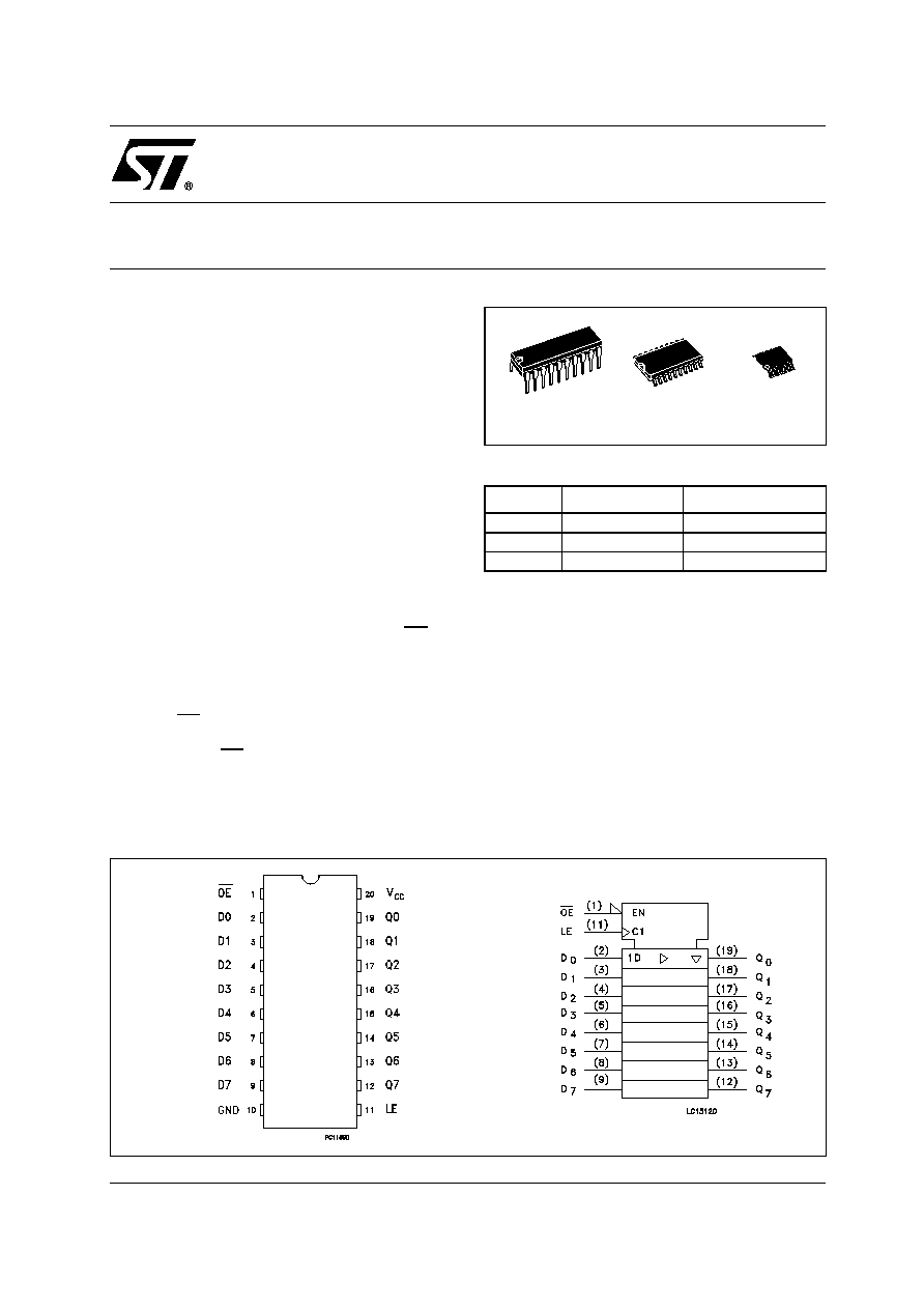
PIN CONNECTION AND IEC LOGIC SYMBOLS
ORDER CODES
PACKAGE
TUBE
T & R
DIP
M74HCT573B1R
SOP
M74HCT573M1R
M74HCT573RM13TR
TSSOP
M74HCT573TTR
TSSOP
DIP
SOP

M74HCT573
2/11
INPUT AND OUTPUT EQUIVALENT CIRCUIT
PIN DESCRIPTION
TRUTH TABLE
X: Don't Care
Z: High Impedance
(*): Q Outputs are latched at the time when the LE input is taken low logic level.
LOGIC DIAGRAM
PIN No
SYMBOL
NAME AND FUNCTION
1
OE
3 State Output Enable
Input (Active LOW)
2, 3, 4, 5, 6,
7, 8, 9
D0 to D7
Data Inputs
12, 13, 14,
15, 16, 17,
18, 19
Q0 to Q7
3 State Latch Outputs
11
LE
Latch Enable Input
10
GND
Ground (0V)
20
V
CC
Positive Supply Voltage
INPUTS
OUTPUTS
OE
LE
D
Q
H
X
X
Z
L
L
X
NO CHANGE (*)
L
H
L
L
L
H
H
H

M74HCT573
3/11
ABSOLUTE MAXIMUM RATINGS
Absolute Maximum Ratings are those values beyond which damage to the device may occur. Functional operation under these conditions is
not implied
(*) 500mW at 65
∞
C; derate to 300mW by 10mW/
∞
C from 65
∞
C to 85
∞
C
RECOMMENDED OPERATING CONDITIONS
Symbol
Parameter
Value
Unit
V
CC
Supply Voltage
-0.5 to +7
V
V
I
DC Input Voltage
-0.5 to V
CC
+ 0.5
V
V
O
DC Output Voltage
-0.5 to V
CC
+ 0.5
V
I
IK
DC Input Diode Current
±
20
mA
I
OK
DC Output Diode Current
±
20
mA
I
O
DC Output Current
±
35
mA
I
CC
or I
GND
DC V
CC
or Ground Current
±
70
mA
P
D
Power Dissipation
500(*)
mW
T
stg
Storage Temperature
-65 to +150
∞C
T
L
Lead Temperature (10 sec)
300
∞C
Symbol
Parameter
Value
Unit
V
CC
Supply Voltage
4.5 to 5.5
V
V
I
Input Voltage
0 to V
CC
V
V
O
Output Voltage
0 to V
CC
V
T
op
Operating Temperature
-55 to 125
∞C
t
r
, t
f
Input Rise and Fall Time (V
CC
= 4.5 to 5.5V)
0 to 500
ns

M74HCT573
4/11
DC SPECIFICATIONS
AC ELECTRICAL CHARACTERISTICS (C
L
= 50 pF, Input t
r
= t
f
= 6ns)
Symbol
Parameter
Test Condition
Value
Unit
V
CC
(V)
T
A
= 25∞C
-40 to 85∞C
-55 to 125∞C
Min.
Typ.
Max.
Min.
Max.
Min.
Max.
V
IH
High Level Input
Voltage
4.5
to
5.5
2.0
2.0
2.0
V
V
IL
Low Level Input
Voltage
4.5
to
5.5
0.8
0.8
0.8
V
V
OH
High Level Output
Voltage
4.5
I
O
=-20
µ
A
4.4
4.5
4.4
4.4
V
I
O
=-6.0 mA
4.18
4.31
4.13
4.10
V
OL
Low Level Output
Voltage
4.5
I
O
=20
µ
A
0.0
0.1
0.1
0.1
V
I
O
=6.0 mA
0.17
0.26
0.33
0.40
I
I
Input Leakage
Current
5.5
V
I
= V
CC
or GND
±
0.1
±
1
±
1
µ
A
I
OZ
High Impedance
Output Leakage
Current
5.5
V
I
= V
IH
or V
IL
V
O
= V
CC
or GND
±
0.5
±
5
±
10
µ
A
I
CC
Quiescent Supply
Current
5.5
V
I
= V
CC
or GND
4
40
80
µ
A
I
CC
Additional Worst
Case Supply
Current
5.5
Per Input pin
V
I
= 0.5V or
V
I
= 2.4V
Other Inputs at
V
CC
or GND
2.0
2.9
3.0
mA
Symbol
Parameter
Test Condition
Value
Unit
V
CC
(V)
C
L
(pF)
T
A
= 25∞C
-40 to 85∞C
-55 to 125∞C
Min.
Typ.
Max.
Min.
Max.
Min.
Max.
t
TLH
t
THL
Output Transition
Time
4.5
50
7
12
15
18
ns
t
PLH
t
PHL
Propagation Delay
Time (LE - Q,Q)
4.5
50
21
33
41
50
ns
4.5
150
25
39
49
59
t
PLH
t
PHL
Propagation Delay
Time (D - Q,Q)
4.5
50
19
30
38
45
ns
4.5
150
23
36
45
54
t
PZL
t
PZH
Output Enable
Time
4.5
50
R
L
= 1 K
19
30
38
45
ns
4.5
150
23
36
45
54
t
PLZ
t
PHZ
Output Disable
Time
4.5
50
R
L
= 1 K
18
25
31
38
ns
t
W(L)
t
W(H)
Minimum Pulse
Width (LE)
4.5
50
7
15
19
22
ns
t
s
Minimum Set-Up
Time
4.5
50
4
10
13
15
ns
t
h
Minimum Hold
Time
4.5
50
5
5
5
ns
M74HCT573
5/11
CAPACITIVE CHARACTERISTICS
1) C
PD
is defined as the value of the IC's internal equivalent capacitance which is calculated from the operating current consumption without
load. (Refer to Test Circuit). Average operating current can be obtained by the following equation. I
CC(opr)
= C
PD
x V
CC
x f
IN
+ I
CC
/8 (per Flip
Flop)
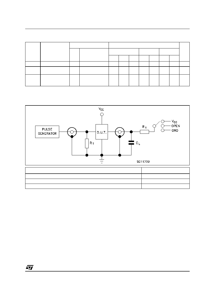
TEST CIRCUIT
C
L
= 50pF/150pF or equivalent (includes jig and probe capacitance)
R
1
= 1K
or equivalent
R
T
= Z
OUT
of pulse generator (typically 50
)
Symbol
Parameter
Test Condition
Value
Unit
V
CC
(V)
T
A
= 25∞C
-40 to 85∞C
-55 to 125∞C
Min.
Typ.
Max.
Min.
Max.
Min.
Max.
C
IN
Input Capacitance
5
10
10
10
pF
C
OUT
Output
Capacitance
10
pF
C
PD
Power Dissipation
Capacitance (note
1)
51
pF
TEST
SWITCH
t
PLH
, t
PHL
Open
t
PZL
, t
PLZ
V
CC
t
PZH
, t
PHZ
GND