
M54HCT688
M74HCT688
February 1993
8 BIT EQUALITY COMPARATOR
B1R
(Plastic Package)
ORDER CODES :
M54HCT688F1R
M74HCT688M1R
M74HCT688B1R
M74HCT688C1R
F1R
(Ceramic Package)
M1R
(Micro Package)
C1R
(Chip Carrier)
PIN CONNECTIONS (top view)
NC =
No Internal
Connection
DESCRIPTION
.
HIGH SPEED
t
PD
= 17 ns (TYP.) AT V
CC
= 5 V
.
LOW POWER DISSIPATION
I
CC
= 4
µ
A (MAX.) AT T
A
= 25
∞
C
.
COMPATIBLE WITH TTL OUTPUTS
V
IH
= 2V (MIN.) V
IL
= 0.8V (MAX)
.
OUTPUT DRIVE CAPABILITY
10 LSTTL LOADS
.
SYMMETRICAL OUTPUT IMPEDANCE
|I
OH
|
=
I
OL
= 4 mA (MIN.)
.
BALANCED PROPAGATION DELAYS
t
PLH
= t
PHL
.
PIN AND FUNCTION COMPATIBLE
WITH 54/74LS688
The M54/74HCT688 utilizes silicon gate C
2
MOS
technology to achieve operating speeds equivalent
to LSTTL devices. Along with the low power
dissipation and high noise immunity of standard
C
2
MOS integrated circuit, it possesses the driving
capability of 10 LSTTL load. The M54/74HCT688
compares bit for bit two 8-bit words applied on inputs
P0 - P7 and inputs Q0 - Q7 and indicates whether
or not they are equal. A single active low enable is
provided to facilitate cascading several packages to
enable comparison of words greater than 8 bits.
This integrated circuit has input and output
characteristics that are fully compatible with 54/74
LSTTL logic families. M54/74HCT devices are
designed to directly interface HSC
2
MOS systems
with TTL and NMOS components. They are also
plug in replacements for LSTTL devices giving a
reduction of power consumption.
All inputs are equipped with protection circuit
against static discharge and transient excess
voltage.
1/10

PIN DESCRIPTION
PIN No
SYMBOL
NAME AND FUNCTION
1
G
Enable Input (Active
LOW)
2, 4, 6, 8,
11, 13, 15,
17
P0 to P7
Word Inputs
3, 5, 7, 9,
12, 14, 16,
18
Q0 to Q7
Word Outputs
19
P = Q
Equal to Output
10
GND
Ground (0V)
20
V
CC
Positive Supply Voltage
IEC LOGIC SYMBOL
ABSOLUTE MAXIMUM RATINGS
Symbol
Parameter
Value
Unit
V
CC
Supply Voltage
-0.5 to +7
V
V
I
DC Input Voltage
-0.5 to V
CC
+ 0.5
V
V
O
DC Output Voltage
-0.5 to V
CC
+ 0.5
V
I
IK
DC Input Diode Current
±
20
mA
I
OK
DC Output Diode Current
±
20
mA
I
O
DC Output Source Sink Current Per Output Pin
±
25
mA
I
CC
or I
GND
DC V
CC
or Ground Current
±
50
mA
P
D
Power Dissipation
500 (*)
mW
T
stg
Storage Temperature
-65 to +150
o
C
T
L
Lead Temperature (10 sec)
300
o
C
Absolute Maximum Ratings are those values beyond which damage to the device may occur. Functional operation under these condition is not implied.
(*) 500 mW:
65
o
C derate to 300 mW by 10mW/
o
C: 65
o
C to 85
o
C
RECOMMENDED OPERATING CONDITIONS
Symbol
Parameter
Value
Unit
V
CC
Supply Voltage
4.5 to 5.5
V
V
I
Input Voltage
0 to V
CC
V
V
O
Output Voltage
0 to V
CC
V
T
op
Operating Temperature: M54HC Series
M74HC Series
-55 to +125
-40 to +85
o
C
o
C
t
r
, t
f
Input Rise and Fall Time (V
CC
= 4.5 to 5.5V)
0 to 500
ns
M54/M74HCT688
3/10
AC ELECTRICAL CHARACTERISTICS (C
L
= 50 pF, Input t
r
= t
f
= 6 ns)
Symbol
Parameter
Test Conditions
Value
Unit
V
CC
(V)
T
A
= 25
o
C
54HC and 74HC
-40 to 85
o
C
74HC
-55 to 125
o
C
54HC
Min.
Typ.
Max.
Min.
Max.
Min.
Max.
t
TLH
t
THL
Output Transition
Time
4.5
8
15
19
22
ns
t
PLH
t
PHL
Propagation
Delay Time
(Pn, Qn - P = Q)
4.5
21
32
40
48
ns
t
PLH
t
PHL
Propagation
Delay Time
(G - P = Q)
4.5
15
23
29
35
ns
C
IN
Input Capacitance
5
10
10
10
pF
C
PD
(*)
Power Dissipation
Capacitance
32
pF
(*) C
PD
is defined as the value of the IC's internal equivalent capacitance which is calculated from the operating current consumption without load.
(Refer to Test Circuit). Average operting current can be obtained by the following equation. I
CC
(opr) = C
PD
∑
V
CC
∑
f
IN
+ I
CC
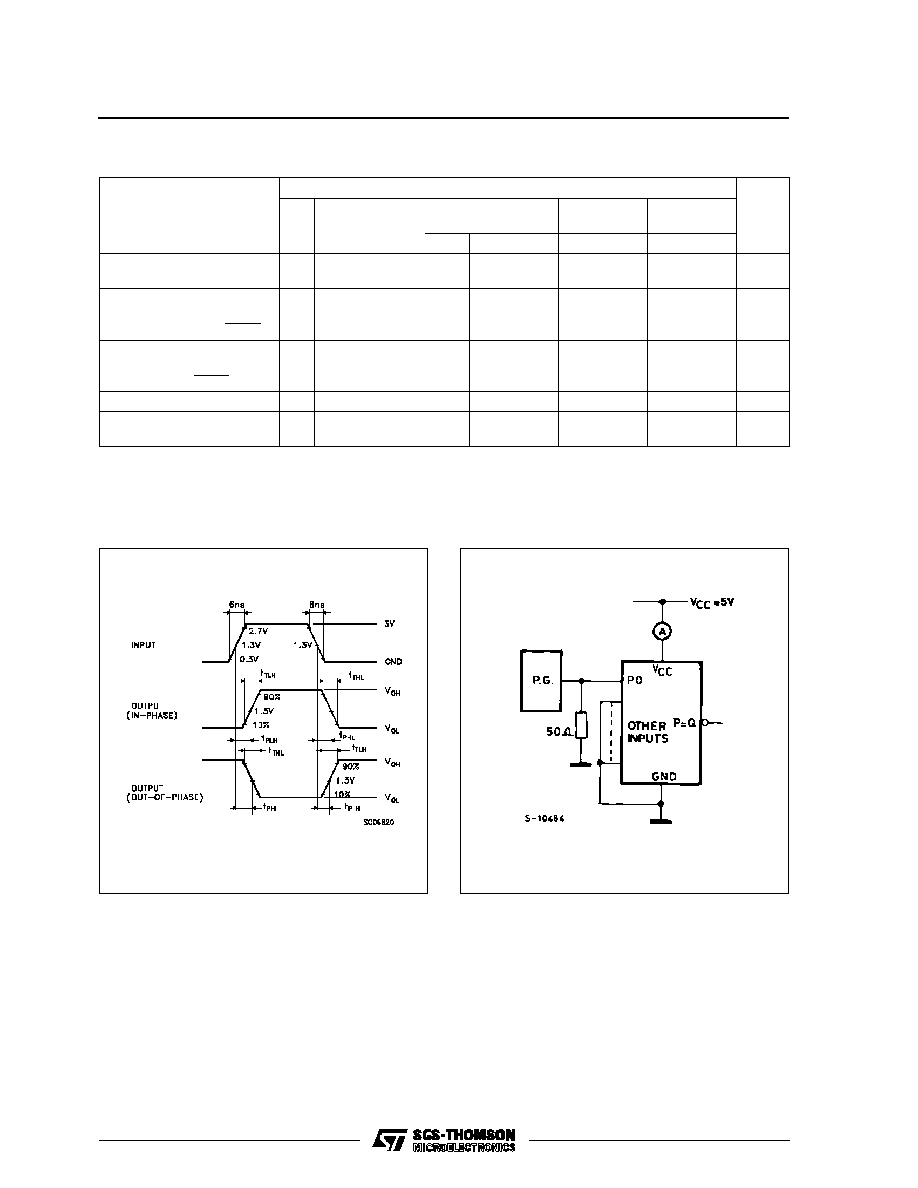
SWITCHING CHARACTERISTICS TEST
WAVEFORM
TEST CIRCUIT ICC (Opr.)
INPUT WAVEFORM IS THE SAME AS THAT IN CASE OF
SWITCHING CHARACTERISTICS TEST.
M54/M74HCT688
5/10

