 | –≠–ª–µ–∫—Ç—Ä–æ–Ω–Ω—ã–π –∫–æ–º–ø–æ–Ω–µ–Ω—Ç: MC1488P | –°–∫–∞—á–∞—Ç—å:  PDF PDF  ZIP ZIP |
MC1488
RS232C QUAD LINE DRIVER
Æ
March 2000
s
CURRENT LIMITED OUTPUT
±
10mA TYP.
s
POWER-OFF SOURCE IMPEDANCE 300
MIN.
s
SIMPLE SLEW RATE CONTROL WITH
EXTERNAL CAPACITOR
s
FLEXIBLE OPERATING SUPPLY RANGE
s
INPUTS ARE TTL AND
µ
P COMPATIBLE
DESCRIPTION
The MC1488 is a monolithic quad line driver
designed to interface data terminal equipment
with
data
communications
equipment
in
conformance with the
specifications of EIA
Standard No. RS232C.
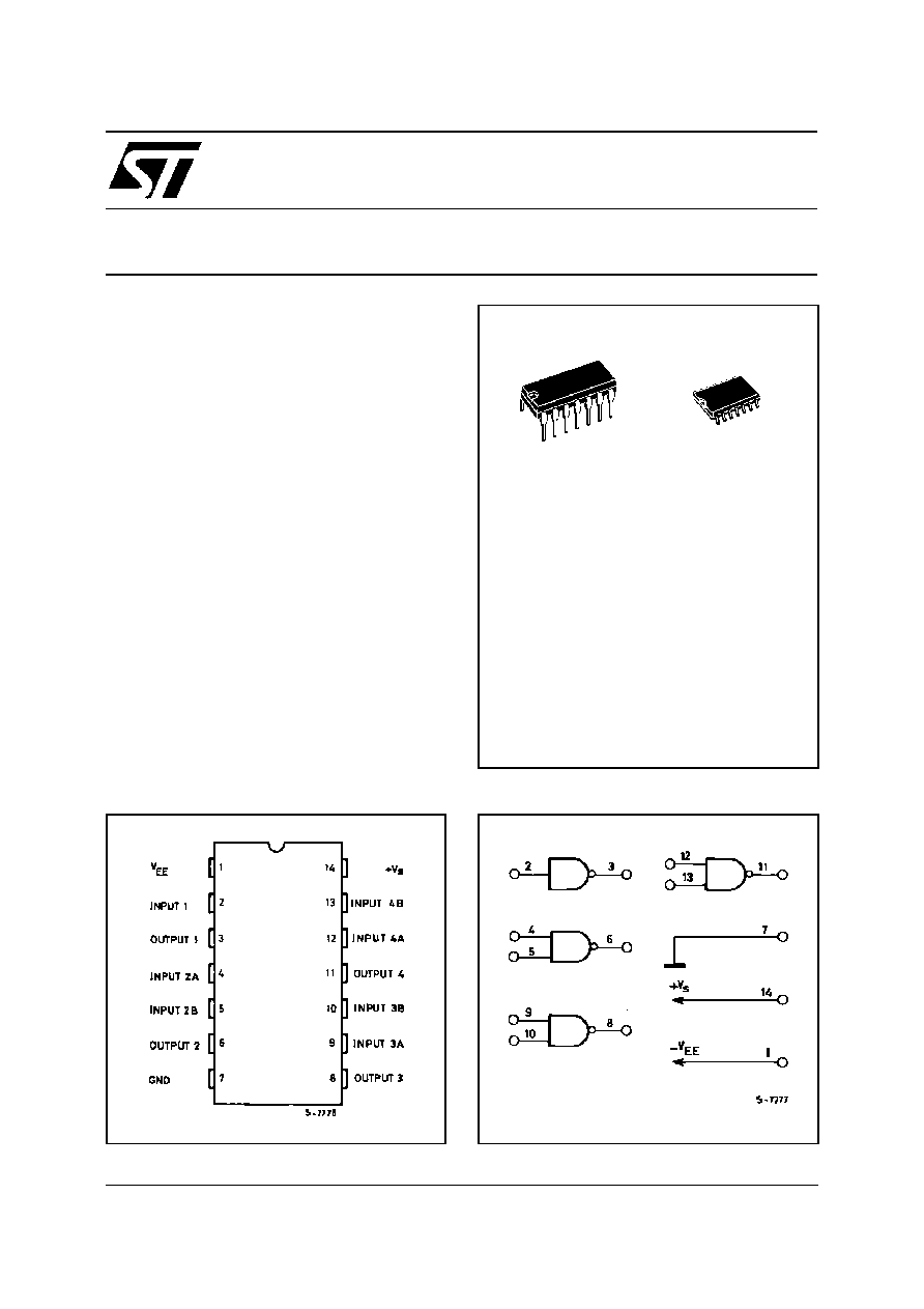
P
DIP14
(Plastic Package)
ORDER CODES :
MC1488P (Plastic DIP)
MC1488D (SO14)
D
SO14
(Plastic Micropackage)
LOGIC DIAGRAM
PIN CONNECTIONS (top view)
1/9

ELECTRICAL CHARACTERISTICS
V
S
= 9
±
10%V, V
E E
= ≠9
±
10%V ,T
amb
= 0 to 75
o
C, unless otherwise specified
Symbo l
Parameter
T est Condi tio ns
Min. Typ . Max. Un it F ig .
I
IL
Input Current
Low Logic StateV
IL
= 0V
1
1.6
mA
1
I
IH
Input Current
High Logic StateV
IH
= 5V
10
µ
A
1
V
OH
Output Voltage
High Logic StateR
L
= 3k
V
IL
= 0.8V, V
S
= 9V, V
EE
= ≠9V
V
IL
= 0.8V, V
S
= 13.2V, V
EE
= ≠13.2V
6
9
7
10.5
V
2
2
V
OL
Output Voltage
Low Logic State
V
IH
= 1.9V, V
EE
= ≠9V, V
S
= 9V
V
IH
= 1.9V, V
EE
= ≠13.2V, V
S
= 13.2V
-6
-9
-7
-10.5
V
2
2
I
OS
+
*
Positive Output Short-circuit
Current
6
10
12
mA
3
I
OS
≠
*
Negative Output Short-circuit
Current
-6
-10
-12
mA
3
R
O
Output Resistance
V
S
= V
EE
= 0V
ol
=
±
2V
300
4
I
s
Positive Supply Current
(R
i
=
)
V
IH
= 1.9V
V
s
= 9V
V
IL
= 0.8V
V
s
= 9V
V
IH
= 1.9V
V
s
= 12V
V
IL
= 0.8V
V
s
= 12V
V
IH
= 1.9V
V
s
= 15V
V
IL
= 0.8V
V
s
= 15V
15
4.5
19
5.5
20
6
25
7
34
12
mA
5
I
EE
Negative Supply Current
(R
L
=
)
V
IH
= 1.9V
V
s
= -9V
V
IL
= 0.8V
V
s
= -9V
V
IH
= 1.9V
V
s
= -12V
V
IL
= 0.8V
V
s
= -12V
V
IH
= 1.9V
V
s
= -15V
V
IL
= 0.8V
V
s
= -15V
-13
-18
-17
-15
-23
-15
-34
-2.5
mA
µ
A
mA
µ
A
mA
mA
5
P
c
Power Consumption
V
S
= 9V
V
EE
= -9V
V
S
= 12V
V
EE
= -12V
333
567
mW
ABSOLUTE MAXIMUM RATINGS
Symbo l
Parameter
T est Cond ition s
Uni t
V
S
Power Supply Voltage
15
V
V
EE
Power Supply Voltage
≠15
V
V
IR
Input Voltage Range
≠15
V
IR
7
V
V
O
Output Signal Voltage
±
15
V
T
amb
Operating Ambient Temperature
0 to 75
o
C
T
stg
Storage Temperature Range
≠65 to 150
o
C
THERMAL DATA
Symbol
Parameter
Pl astic DIP14 Ceramic DIP14
SO14
R
th j-amb
Thermal Resistance Junction-ambientMax.
200
o
C/W
165
o
C/W
165
o
C/W
SWITCHING CHARACTERISTICS V
S
=
±
9
±
1V, V
E E
= ≠9
±
1%V ,T
amb
= 25
o
C
Symb ol
Parameter
Test Co nditi ons
Mi n. T yp. Max. Uni t F ig.
t
PHL
Propagation Delay Time
Z
i
= 3k
and 15pF
275
350
ns
6
t
THL
Fall Time
Z
i
= 3k
and 15pF
45
75
ns
6
t
PHL
Propagation Delay Time
Z
i
= 3k
and 15pF
110
175
ns
6
t
THL
Rise Time
Z
i
= 3k
and 15pF
55
100
ns
6
* Maximum package power dissipation may be exceeded if all outputs are shorted simultaneously.
MC1488
2/9

TEST CIRCUITS
Figure 1 : Input Current
Figure 3 : Output Short-Circuit Current
Figure 5 : Power Supply Currents
Figure 2 : Output Voltage
Figure 4 : Output Resistance (power off)
Figure 6 : Switching Response
MC1488
3/9

Figure 7 : Transfer Characteristics versus
Figure 8 : Short-Circuit Output Current versus
Temperature
Figure 9 : Output Slew-Rate Load Capacitance
Figure 10 : Output Voltage and Current Limiting
Characteristics
Figure 11 : Maximum Operating Temperature
versus Power Supply Voltage
MC1488
4/9

TYPICAL APPLICATION : RS232C Data Transmission
The Electronic Industries Association (EIA) has
released the RS232C specification detailing the
requirements for the interface between data
processing equipment. This standard specifies
not only the number and type of interface leads,
but also the voltage levels to be used. The
MC1488 quad driver and its companion circuit,
the MC1489 quad receiver, provide a complete
interface system between DTL or TTL logic levels
and the RS232C defined levels. The RS232C
requirements as applied to drivers are discussed
herein.
The required driver voltages are defined as
between 5 and 15 V in magnitude and are
positive for a logic "0" and negative for a logic "1".
These voltages are so defined when the drivers
are terminated with a 3000 to 7000
resistor.
The MC1488 meets this voltage requirement by
converting a DTL/TTL logic level into RS232C
levels with one stage of inversion.
The RS232C specification further requires that
during transitions, the driver output slew rate
must not exceed 30 V per
µ
s. The inherent slew
rate of the MC1488 is much too fast for this
requirement. The current limited output of the
device can be used to control this slew rate by
connecting a capacitor to each driver output. The
required capacitor can be easily determined by
using the relationship C = I
OS
x
T/
V from
which Figure 12 is derived. Accordingly, a 330 pF
capacitor on each output will guarantee a worst
case slew rate of 30 V per
µ
s.
The interface driver is also required to withstand
an accidental short to any other conductor in an
interconnecting cable. The worst possible signal
on any conductor would be another driver using a
plus or minus 15 V, 500 mA source. The MC1488
is designed to indefinitely withstand such a short
to all four outputs in a package as long as the
power-supply voltages are greater than 9.0 V
(i.e., VS
9.0 V ; V
EE
- 9.0 V). In some
power-supply designs, a loss of system power
causes a low impedance on the power-supply
outputs. When this occurs, a low impedance to
ground would exist at the power inputs to the
MC1488 effectively shorting the 300
output
resistor to ground. If all four outputs were then
shorted to plus or minus 15 V, the power
dissipation in these resistors would be excessive.
Therefore, if the system is designed to permit low
impedances to ground at the power-suppies of
the drivers, a diode should be placed in each
power-supply lead to prevent over-heating in this
fault condition. These two diodes, as shown in
Figure 13, could be used to decouple all the
driver packages in a system. (These same diodes
will allow the MC1488 to withstand momentary
shorts to the
±
15 V limits specified in the earlier
APPLICATION INFORMATION
MC1488
5/9

Standard RS232B). The addition of the diodes
also permits the MC1488 to withstand faults with
power-supplies of less than the 9.0 V stated
above.
The maximum short-circuit current allowable
under fault conditions is more than guaranteed by
the previously mentioned 10 mA output current
limiting.
The MC1488 is an extremely versatile line driver
with a miriad of possible applications. Several
features of the drivers enhance this versatility :
1. Output Current Limiting - this enables the
circuit designer to define the ouptut voltage levels
independent of power-supplies and can be
accomplished by diode clamping of the output
pins.
2. Power-Supply Range - as can be seen from
the schematic drawing of the drivers, the positive
and negative driving elements of the device are
essentially independent and do not
require
matching power-supplies. In fact, the positive
supply can very from a minimum seven volts
(required for
driving the
negative pulldown
section) to the maximum specified 15 V. The
negative supply can vary from approximately -
2.5 V to the minimum specified - 15 V. The
MC1488 will drive the ouptut to within 2 V of the
positive or negative supplies as long as the
current output limits are not exceeded. The
combination
of
the
current-limiting
and
supply-voltage features allow a wide combination
of possible outputs within the same quad
package.
Figure 12 : Slew Rate versus Capacitance for
I
sc
= 10mA
Figure 13 : Power Supply Protection to Meet
Power-off Fault Conditions
MC1488
6/9

DIM.
mm
inch
MIN.
TYP.
MAX.
MIN.
TYP.
MAX.
a1
0.51
0.020
B
1.39
1.65
0.055
0.065
b
0.5
0.020
b1
0.25
0.010
D
20
0.787
E
8.5
0.335
e
2.54
0.100
e3
15.24
0.600
F
7.1
0.280
I
5.1
0.201
L
3.3
0.130
Z
1.27
2.54
0.050
0.100
P001A
Plastic DIP-14 MECHANICAL DATA
MC1488
7/9

DIM.
mm
inch
MIN.
TYP.
MAX.
MIN.
TYP.
MAX.
A
1.75
0.068
a1
0.1
0.2
0.003
0.007
a2
1.65
0.064
b
0.35
0.46
0.013
0.018
b1
0.19
0.25
0.007
0.010
C
0.5
0.019
c1
45 (typ.)
D
8.55
8.75
0.336
0.344
E
5.8
6.2
0.228
0.244
e
1.27
0.050
e3
7.62
0.300
F
3.8
4.0
0.149
0.157
G
4.6
5.3
0.181
0.208
L
0.5
1.27
0.019
0.050
M
0.68
0.026
S
8 (max.)
P013G
SO-14 MECHANICAL DATA
MC1488
8/9

Information furnished is believed to be accurate and reliable. However, STMicroelectronics assumes no responsibility for the consequences
of use of such information nor for any infringement of patents or other rights of third parties which may result from its use. No license is
granted by implication or otherwise under any patent or patent rights of STMi croelectronics. Specification mentioned in this publication are
subject to change without notice. This publication supersedes and replaces all information previously supplied. STMi croelectronics products
are not authorized for use as critical components in life support devices or systems withoutexpress written approval of STMicroelectronics.
The ST logo is a registered trademark of STMicroelectronics
©
2000 STMicroelectronics ≠ Printed in Italy ≠ All Rights Reserved
STMicroelectronics GROUP OF COMPANIES
Australia - Brazil - China - Finland - France - Germany - Hong Kong - India - Italy - Japan - Malaysia - Malta - Morocco
Singapore - Spain - Sweden - Switzerland - United Kingdom - U.S.A.
http://www.st.com
.
MC1488
9/9