 | –≠–ª–µ–∫—Ç—Ä–æ–Ω–Ω—ã–π –∫–æ–º–ø–æ–Ω–µ–Ω—Ç: MC1489P | –°–∫–∞—á–∞—Ç—å:  PDF PDF  ZIP ZIP |

1/13
September 2003
s
INPUT RESISTANCE ≠3k to 7k
s
INPUT SIGNAL RANGE ≠ ± 30V
s
INPUT THRESHOLD HYSTERESIS BUILT-IN
s
RESPONSE CONTROL:
a) LOGIC THRESHOLD SHIFTING
b) INPUT NOISE FILTERING
DESCRIPTION
The MC1489 monolithic quad line receivers are
designed to interface data terminal equipment
with
data
communications
equipment
in
conformance
with
the
specifications
of
EIA
Standard N∞ RS232C.
SCHEMATIC DIAGRAM
MC1489
MC1489A
QUAD LINE RECEIVERS
DIP
SOP

MC1489/MC1489A
2/13
PIN CONFIGURATION (top view)
ORDERING CODES
ABSOLUTE MAXIMUM RATINGS
Absolute Maximum Ratings are those values beyond which damage to the device may occur. Functional operation under these condition is
not implied.
DIP14
SO14
SO14 (TAPE & REEL)
MC1489P
MC1489D1
MC1489D1013TR
MC1489AP
MC1489AD1013TR
Symbol
Parameter
Value
Unit
V
S
Power Supply Voltage
10
V
V
I
Input Voltage Range
±
30
V
I
OL
Output Load Current
20
mA
P
TOT
Power Dissipation
1
W
T
amb
Operating Ambient Temperature
0 to 75
∞C
T
stg
Storage Temperature Range
-65 to 150
∞C

MC1489/MC1489A
3/13
ELECTRICAL CHARACTERISTICS
Response Control Pin in Open; V
S
= 5V, T
amb
= 0 to 75∞C, unless otherwise specified.
SWITCHING CHARACTERISTICS
V
S
= 5V, T
amb
= 25∞C, (see Figure 1)
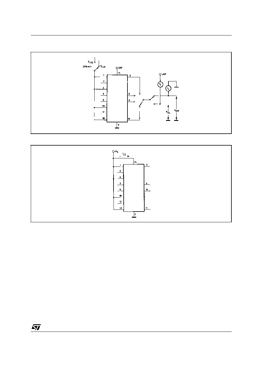
TEST CIRCUITS
Figure 1 : Switching Response
Symbol
Parameter
Test Conditions
Min.
Typ.
Max.
Unit
I
IH
Positive Input Current
V
IH
= 25 V
3.6
8.3
mA
V
IH
= 3 V
0.43
I
IL
Negative Input Current
V
IL
= - 25 V
-3.6
-8.3
mA
V
IL
= - 3 V
-0.43
V
IH
Input Turn-On Threshold
Voltage
T
amb
= 25∞C, V
OL
0.45 V
I
L
= 10 mA
for MC1489
1
1.5
V
for MC1489A
1.75
1.95
2.25
V
IL
Input Turn-Off Threshold
Voltage
T
amb
= 25∞C, V
OL
2.5 V I
L
= -0.5 mA
0.75
1.25
V
V
OH
Output Voltage High
V
IH
= 0.75 V, I
L
= -0.5 mA
2.5
4
5
V
I
L
= 0.5 mA Input Open Circuit
2.5
4
5
V
OL
Output Voltage Low
V
IL
= 3 V, I
L
= 10 mA
0.2
0.45
V
I
OS
Output Short Circuit
Current
-3
-4
mA
I
S
Power Supply Current
All gates "ON", I
O
= 0 mA, V
IH
= 5 V
16
26
mA
P
C
Power Consumption
V
IH
= 5 V
80
130
mW
Symbol
Parameter
Test Conditions
Min.
Typ.
Max.
Unit
t
PLH
Propagation Delay Time
R
L
= 3.9 K
25
85
ns
t
THL
Rise Time
R
L
= 3.9 K
120
175
ns
t
PHL
Propagation Delay Time
R
L
= 390
25
50
ns
t
THL
Fall Time
R
L
= 390
10
20
ns

MC1489/MC1489A
4/13
Figure 2 : Response Control Node
Figure 3 : Input Current
Figure 4 : Output Short-Circuit Current
C: capacitor is for noise filtering
MC1489/MC1489A
5/13
Figure 5 : Output Voltage and Input Threshold Voltage
Figure 6 : Power Supply Currents