 | –≠–ª–µ–∫—Ç—Ä–æ–Ω–Ω—ã–π –∫–æ–º–ø–æ–Ω–µ–Ω—Ç: MC3403P | –°–∫–∞—á–∞—Ç—å:  PDF PDF  ZIP ZIP |

Æ
.
SHORT-CIRCUIT PROTECTED OUTPUTS
.
CLASS AB OUTPUT STAGE FOR MINIMAL
CROSSOVER DISTORTION
.
SINGLE SUPPLY OPERATION : + 3 V TO + 36V
.
DUAL SUPPLIES :
±
1.5V TO
±
18V
.
LOW INPUT BIAS CURRENT : 500nA MAX
.
INTERNALLY COMPENSATED
.
SIMILAR PERFORMANCE TO POPULAR
UA741
DESCRIPTION
The MC3403 is a low-cost, quad operational ampli-
fier with true differential inputs. The device has elec-
trical characteristics similar to the popular UA741.
However the MC3403, has several distinct advan-
tages over standard operational amplifier types in
single supply applications. The quad amplifier can
operate at supply voltages as low as 3.0 volts or as
high as 36 volts with quiescent currents about one
third of those associated with the UA741 (on a per
amplifier basis). The common-mode input range in-
cludes the negative supply, thereby eliminating the
necessity for external biasing components in many
applications.
Inverting Input 2
Non-inverting Input 2
Non-inverting Input 1
CC
V
-
CC
V
1
2
3
4
8
5
6
7
9
10
11
12
13
14
+
Output 3
Output 4
Non-inverting Input 4
Inverting Input 4
Non-inverting Input 3
Inverting Input 3
-
+
-
+
-
+
-
+
Output 1
Inverting Input 1
Output 2
PIN CONNECTIONS (top view)
ORDER CODES
Part
Number
Temperature
Range
Package
N
D
P
MC3303
≠40
o
C, +105
o
C
∑
∑
∑
MC3403
0
o
C, +70
o
C
∑
∑
∑
MC3503
≠55
o
C, +125
o
C
∑
∑
∑
Example : MC3403N
LOW POWER QUAD BIPOLAR OPERATIONAL AMPLIFIERS
MC3303
MC3403 - MC3503
August 1998
N
DIP14
(Plastic Package)
D
SO14
(Plastic Micropackage)
P
TSSOP14
(Thin Shrink Small Outline Package)
1/11

ABSOLUTE MAXIMUM RATINGS
Symbol
Parameter
MC3503
MC3403
MC3303
Unit
V
CC
Supply Voltage
±
18 or 36
±
18 or 36
±
18 or 36
V
V
id
Differential Input Voltage
±
36
±
36
±
36
V
V
i
Input Voltage (note 1)
±
18
±
18
±
18
V
≠
Output Short-circuit Duration (note 2)
Infinite
≠
P
tot
Power Dissipation
500
500
500
mW
T
oper
Operating Free-air Temperature Range
≠55 to +125
0 to +70
≠40 to +105
o
C
T
stg
Storage Temperature Range
≠65 to +150
≠65 to +150
≠65 to +150
o
C
Notes :
1. For supply voltages less than
±
15V, the absolute maximum input voltage is equal to the supply voltage.
2. Any of the amplifier outputs can be shorted to ground indefinitely ; however more than one should not be simultaneously shorted
as the maximum junction temperature will be exceeded.
(1 stage)
Q20
Q23
8pF
C1
Q19
Q18
Q17
Q16
Output
Q27
V
CC
Q29
Q28
Q15
R3
25
Q30
R5
8.2k
V
CC
(Ground)
Q12
Q11
Q10
Q13
R2
37 k
R4
31k
R6
0.7k
Q9
Q8
Q7
Q6
Q14
R1
12k
Q4
Q3
Q2
Q21
Q22
Q24
Q25
Non-inverting
input
input
Inverting
Q5
Q1
SCHEMATIC DIAGRAM (each amplifier)
V
CC
V
CC
+3V to +30V
SINGLE SUPPLY
1.5V to 18V
1.5V to 18V
V
CC
V
CC
DUAL SUPPLIES
MC3303 - MC3403 - MC3503
2/11
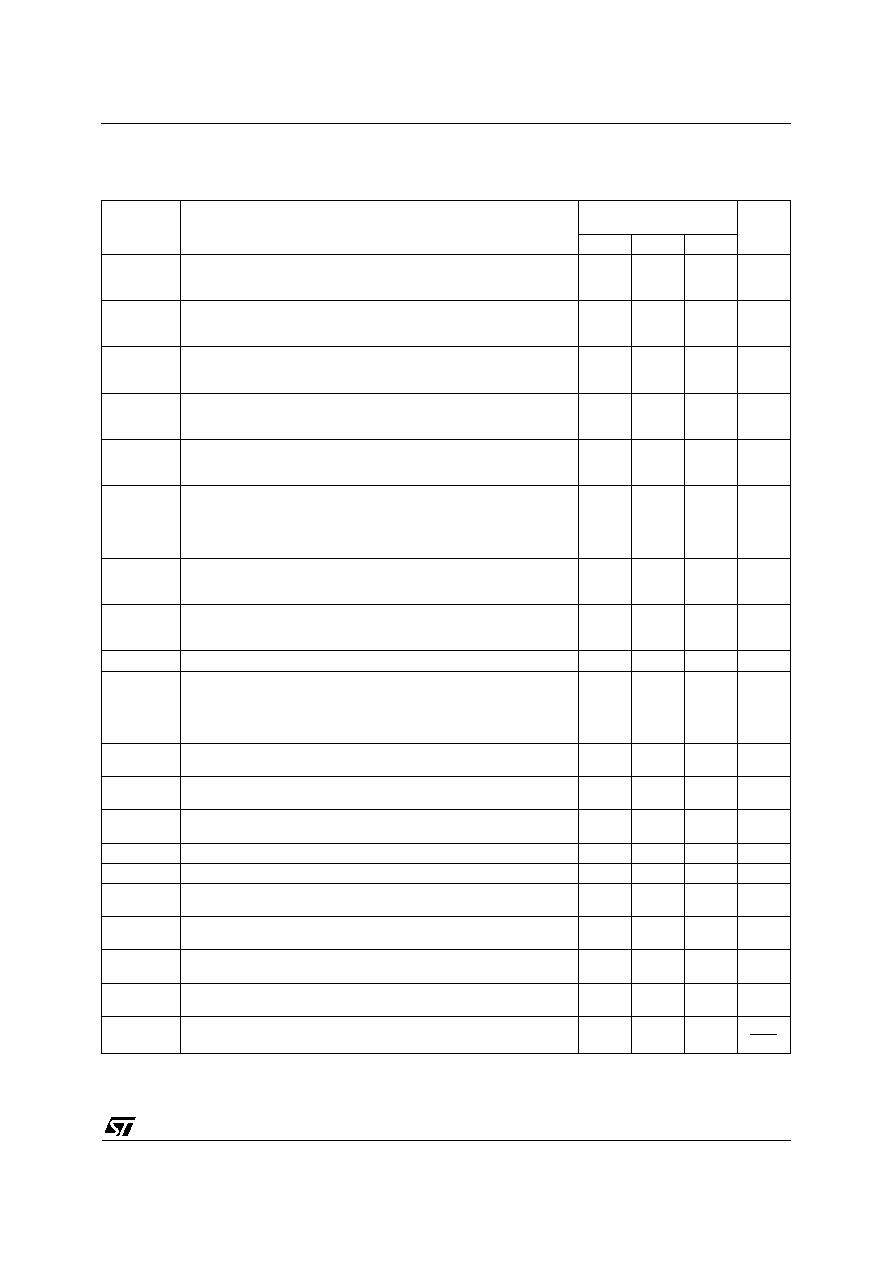
ELECTRICAL CHARACTERISTICS
V
CC
=
±
15V, T
amb
= +25
o
C, (unless otherwise specified)
Symbol
Parameter
MC3303 - MC3403
MC3503
Unit
Min.
Typ.
Max.
V
IO
Input Offset Voltage (R
S
10k
)
T
amb
= 25
o
C
T
min.
T
amb
T
max.
1
5
6
mV
I
IO
Input Offset Current
T
amb
= 25
o
C
T
min.
T
amb
T
max.
2
50
200
nA
I
ib
Input Bias Current
T
amb
= 25
o
C
T
min.
T
amb
T
max.
40
500
800
nA
A
vd
Large Signal Voltage Gain (V
O
=
±
10V, R
L
= 2k
)
T
amb
= 25
o
C
T
min.
T
amb
T
max.
50
25
200
V/mV
SVR
Supply Voltage Rejection Ratio (R
S
10k
)
T
amb
= 25
o
C
T
min.
T
amb
T
max.
77
77
90
dB
I
CC
Supply Current, all Amp, no Load
T
amb
= 25
o
C
MC3503
T
min.
T
amb
T
max.
MC3503
2.8
7
4
8
5
mA
V
icm
Input Common Mode Voltage Range
T
amb
= 25
o
C
T
min.
T
amb
T
max.
≠ 15
≠ 15
+ 13
+ 13
V
CMR
Common Mode Rejection Ratio (R
S
10k
)
T
amb
= 25
o
C
T
min.
T
amb
T
max.
70
70
90
dB
I
OS
Output Short-circuit Current
10
30
45
mA
±
V
opp
Output Voltage Swing
T
amb
= 25
o
C
R
L
= 10k
R
L
= 2k
T
min.
T
amb
T
max.
R
L
= 2k
R
L
= 10k
12
10
10
12
13.5
13
V
SR
Slew Rate (V
I
=
±
10V R
L
= 2k
, C
L
= 100pF,
T
amb
= 25
o
C, unity gain)
0.35
0.5
V/
µ
s
t
r
, t
f
Rise Time and Fall Time (V
O
=
±
20mV, R
L
= 2k
, C
L
= 100pF
T
amb
= 25
o
C, unity gain)
0.18
µ
s
K
OV
Overshoot (V
I
=
±
20mV, R
L
= 2k
, C
L
= 100pF,
T
amb
= 25
o
C, unity gain)
10
%
Z
I
Input Impedance
0.3
1
M
Z
O
Output Impedance
75
B
om
Power Bandwidth (R
L
= 2k
, C
L
= 100pF, A
v
= 1, T
amb
= 25
o
C,
V
O
= 2V
pp
, THD
5%)
9
kHz
B
Unity Gain Bandwidth (V
O
= 10mV, R
L
= 2k
, C
L
= 100pF,
T
amb
= 25
o
C, unity gain)
1
MHz
GBP
Gain Bandwidth Product (V
O
= 10mV, R
L
= 2k
, C
L
= 100pF,
f = 100kHz, T
amb
= 25
o
C)
0.7
1
MHz
THD
Total Harmonic Distortion (f = 1kHz, A
v
= 20dB, R
L
= 2k
,
V
O
= 2V
pp
, C
L
= 100pF, T
amb
= 25
o
C)
0.02
%
e
n
Equivalent Input Noise Voltage (f = 1kHz, R
s
= 100
)
43
nV
Hz
MC3303 - MC3403 - MC3503
3/11

ELECTRICAL CHARACTERISTICS (continued)
Symbol
Parameter
MC3303 - MC3403 - MC3503
Unit
Min.
Typ.
Max.
m
Phase Margin
60
Degrees
DV
IO
Input Offset Voltage Drift
T
min.
T
amb
T
max.
10
µ
V/
o
C
DI
IO
Input Offset Current Drift
T
min
.
T
amb
25
o
C
50
pA/
o
C
V
O1
/V
02
Channel Separation
120
dB
ELECTRICAL CHARACTERISTICS
V
CC
+
= 5V, V
CC
≠
= Ground, T
amb
= 25
o
C (unless otherwise specified)
Symbol
Parameter
MC3303 - MC3403 - MC3503
Unit
Min.
Typ.
Max.
V
IO
Input Offset Voltage (R
S
10k
)
T
amb
= 25
∞
C
T
min
T
amb
T
max
1
5
6
mV
I
IO
Input Offset Current
T
amb
= 25
o
C
T
min.
T
amb
T
max.
2
50
200
nA
I
ib
Input Bias Current
T
amb
= 25
o
C
T
min.
T
amb
T
max.
40
500
800
nA
A
vd
Large Signal Voltage Gain (V
O
= 1.4 to 2.4V, R
L
= 2k
)
T
amb
= 25
o
C
T
min.
T
amb
T
max.
10
5
200
V/mV
SVR
Supply Voltage Rejection Ratio (R
S
10k
)
T
amb
= 25
o
C
T
min.
T
amb
T
max.
77
77
90
dB
I
CC
Supply Current (All Amp)
MC3503
2.5
7
4
mA
V
opp
Output Voltage Range (R
L
= 10k
)
V
CC
= +5V
+5 < V
CC
+30V
3.3
V
CC
+
-2V
3.5
V
CC
+
-1.7V
V
MC3303 - MC3403 - MC3503
4/11

The MC3403 is made using four internally compen-
sated, two-stage operational amplifiers. The first
stage of each consists of differential input devices
Q24 and Q22 with input buffer transistors Q25 and
Q21 and the differential to single ended converter
Q3 and Q4. The first stage performs not only the first
stage gain function but also performs the level shift-
ing and transconductance reduction functions. By
reducing the transconductance a smaller compen-
sation capacitor (only 8pF) can be employed, thus
saving chip area.
The transconductance reduction is accomplished
by splitting the collectors of Q24 and Q22. Another
feature of this input stage is that the input common-
mode range can include the negative supply of
ground, in single supply operation, without satura-
tion either the input devices or the differential to sin-
gle-ended converter.
The second stage consists of a standard current
source load amplifier stage. The output stage is
unique because it allows the output to swing to
ground in single supply operation and yet does not
exhibit any crossover distortion in split supply opera-
tions. This is possible because class AB operation
is utilized.
Each amplifier is biased from an internal voltage
regulator which has a low temperature coefficient
thus giving each amplifier good temperature charac-
teristics as well as excellent power supply rejection.
CIRCUIT DESCRIPTION
20
µ
s/div.
TYPICAL PERFORMANCE CURVES
A
V
= 100
1/4
MC3403
V
O
V
CC
V
CC
R1
10k
V
O
=
V
CC
1
2
V
O
R1
R1 + R2
V
CC
=
R2
10k
APPLICATION INFORMATION
VOLTAGE REFERENCE
50k
5k
10k
1/4
MC3403
V
O
V
CC
V
(ref)
R
C
C
R
V
(ref)
= 1
2
V
CC
f
O
=
1
2
RC
For
f
O
= 1kHz
R = 16k
C = 0.01
µ
F
WIEN BRIDGE OSCILLATOR
MC3303 - MC3403 - MC3503
5/11