 | –≠–ª–µ–∫—Ç—Ä–æ–Ω–Ω—ã–π –∫–æ–º–ø–æ–Ω–µ–Ω—Ç: MJD32CT4 | –°–∫–∞—á–∞—Ç—å:  PDF PDF  ZIP ZIP |

MJD31B/31C
MJD32B/32C
COMPLEMENTARY SILICON POWER TRANSISTORS
s
STMicroelectronics PREFERRED
SALESTYPES
s
SURFACE-MOUNTING TO-252 (DPAK)
POWER PACKAGE IN TAPE & REEL
(SUFFIX "T4")
s
ELECTRICALLY SIMILAR TO TIP31B/C AND
TIP32B/C
APPLICATIONS
s
GENERAL PURPOSE SWITCHING AND
AMPLIFIER TRANSISTORS
DESCRIPTION
The MJD31B and MJD31C and the MJD32B and
MJD32C form complementary NPN-PNP pairs.
They are manufactured using Epitaxial Base
technology for cost-effective performance.
Æ
INTERNAL SCHEMATIC DIAGRAM
May 1999
1
3
DPAK
TO-252
(Suffix "T4")
ABSOLUTE MAXIMUM RATINGS
Symbol
Parameter
Value
Unit
NPN
MJD31B
MJD31C
PNP
MJD32B
MJD32C
V
CBO
Collector-Base Voltage (I
E
= 0)
80
100
V
V
CEO
Collector-Emitter Voltage (I
B
= 0)
80
100
V
V
EBO
Emitter-Base Voltage (I
C
= 0)
5
V
I
C
Collector Current
3
A
I
CM
Collector Peak Current
5
A
I
B
Base Current
1
A
P
tot
Total Dissipation at T
c
= 25
o
C
15
W
T
stg
Storage Temperature
-65 to 150
o
C
T
j
Max. Operating Junction Temperature
150
o
C
For PNP types the values are intented negative.
1/5
THERMAL DATA
R
thj-case
R
thj-amb
Thermal Resistance Junction-case Max
Thermal Resistance Junction-ambient Max
8.33
100
o
C/W
o
C/W
ELECTRICAL CHARACTERISTICS (T
case
= 25
o
C unless otherwise specified)
Symbol
Parameter
Test Conditions
Min.
Typ.
Max.
Unit
I
CES
Collector Cut-off
Current (V
BE
= 0)
V
CE
= Max Rating
20
µ
A
I
CEO
Collector Cut-off
Current (I
B
= 0)
V
CE
= 60 V
50
µ
A
I
EBO
Emitter Cut-off Current
(I
C
= 0)
V
EB
= 5 V
0.1
mA
V
CEO(sus)
Collector-Emitter
Sustaining Voltage
I
C
= 30 mA
for MJD31B/32B
for MJD31C/32C
80
100
V
V
V
CE(sat)
Collector-Emitter
Saturation Voltage
I
C
= 3 A I
B
= 375 mA
1.2
V
V
BE(on)
Base-Emitter Voltage
I
C
= 3 A V
CE
= 4 V
1.8
V
h
FE
DC Current Gain
I
C
= 1 A V
CE
= 4 V
I
C
= 3 A V
CE
= 4 V
25
10
50
h
fe
Dynamic Current Gain
I
C
= 0.5 A V
CE
= 10 V f = 1 KHz
I
C
= 0.5 A V
CE
= 10 V f = 1 MHz
20
3
Pulsed: Pulse duration = 300
µ
s, duty cycle
2 %
For PNP type voltage and current values are negative.
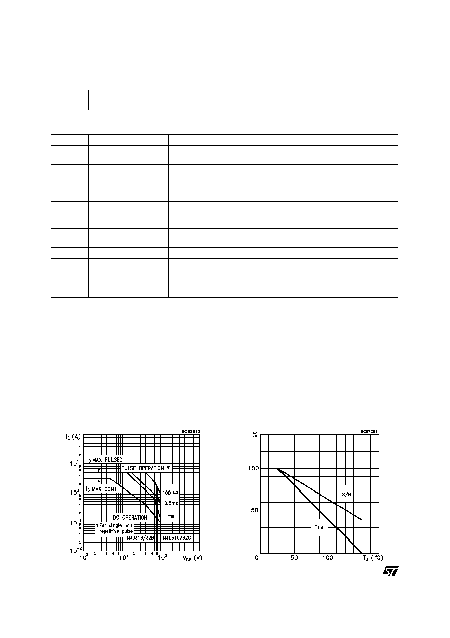
Safe Operating Area
Derating Curves
MJD31B/31C - MJD32B/32C
2/5

DC Current Gain (NPN type)
Collector-Emitter Saturation Voltage (NPN type)
Base-Emitter Saturation Voltage (NPN type)
DC Current Gain (PNP type)
Collector-Emitter Saturation Voltage (PNP type)
Collector-Base Capacitance (PNP type)
MJD31B/31C - MJD32B/32C
3/5

DIM.
mm
inch
MIN.
TYP.
MAX.
MIN.
TYP.
MAX.
A
2.20
2.40
0.087
0.094
A1
0.90
1.10
0.035
0.043
A2
0.03
0.23
0.001
0.009
B
0.64
0.90
0.025
0.035
B2
5.20
5.40
0.204
0.213
C
0.45
0.60
0.018
0.024
C2
0.48
0.60
0.019
0.024
D
6.00
6.20
0.236
0.244
E
6.40
6.60
0.252
0.260
G
4.40
4.60
0.173
0.181
H
9.35
10.10
0.368
0.398
L2
0.8
0.031
L4
0.60
1.00
0.024
0.039
V2
0
o
8
o
0
o
0
o
P032P_B
TO-252 (DPAK) MECHANICAL DATA
MJD31B/31C - MJD32B/32C
4/5

Information furnished is believed to be accurate and reliable. However, STMicroelectronics assumes no responsibility for the consequences
of use of such information nor for any infringement of patents or other rights of third parties which may result from its use. No license is
granted by implication or otherwise under any patent or patent rights of STMicroelectronics. Specification mentioned in this publication are
subject to change without notice. This publication supersedes and replaces all information previously supplied. STMicroelectronics products
are not authorized for use as critical components in life support devices or systems without express written approval of STMicroelectronics.
The ST logo is a trademark of STMicroelectronics
© 1999 STMicroelectronics ≠ Printed in Italy ≠ All Rights Reserved
STMicroelectronics GROUP OF COMPANIES
Australia - Brazil - Canada - China - France - Germany - Italy - Japan - Korea - Malaysia - Malta - Mexico - Morocco - The Netherlands -
Singapore - Spain - Sweden - Switzerland - Taiwan - Thailand - United Kingdom - U.S.A.
http://www.st.com
.
MJD31B/31C - MJD32B/32C
5/5