 | –≠–ª–µ–∫—Ç—Ä–æ–Ω–Ω—ã–π –∫–æ–º–ø–æ–Ω–µ–Ω—Ç: MSC83303 | –°–∫–∞—á–∞—Ç—å:  PDF PDF  ZIP ZIP |

STPS20L15D/G
Æ
July 1999 - Ed: 2B
LOW DROP OR-ing POWER SCHOTTKY DIODE
I
F(AV)
20 A
V
RRM
15 V
Tj (max)
125∞C
V
F
(max)
0.33 V
MAIN PRODUCT CHARACTERISTICS
VERY LOW FORWARD VOLTAGE DROP FOR
LESS POWER DISSIPATION AND REDUCED
HEATSINK SIZE
REVERSE VOLTAGE SUITED TO OR-ing OF 3V,
5V and 12V RAILS
FEATURES AND BENEFITS
Packaged in TO-220AC or D
2
PAK, this device is
especially intended for use as an OR-ing diode in
fault tolerant power supply equipments.
DESCRIPTION
TO-220AC
STPS20L15D
A
K
K
Symbol
Parameter
Value
Unit
V
RRM
Repetitive peak reverse voltage
15
V
I
F(RMS)
RMS forward current
30
A
I
F(AV)
Average forward current
Tc = 115∞C
= 1
20
A
I
FSM
Surge non repetitive forward current
tp = 10 ms
Sinusoidal
310
A
I
RRM
Repetitive peak reverse current
tp = 2
µ
s F = 1kHz
2
A
I
RSM
Non repetitive peak reverse current
tp = 100
µ
s
3
A
T
stg
Storage temperature range
- 65 to + 150
∞
C
Tj
Maximum operating junction temperature *
125
∞
C
dV/dt
Critical rate of rise of reverse voltage
10000
V/
µ
s
ABSOLUTE RATINGS (limiting values)
D
2
PAK
STPS20L15G
NC
A
K
* :
dPtot
dTj
<
1
Rth
(
j
-
a
)
thermal runaway condition for a diode on its own heatsink
1/5

Symbol
Parameter
Value
Unit
R
th (j-c)
Junction to case
1.6
∞
C/W
THERMAL RESISTANCES
Symbol
Tests Conditions
Tests Conditions
Min.
Typ.
Max.
Unit
I
R
*
Reverse leakage
current
Tj = 25
∞
C
V
R
= 15V
6
mA
Tj = 100
∞
C
V
R
= 15V
200
500
V
F
*
Forward voltage drop
Tj = 25
∞
C
I
F
= 19 A
0.41
V
Tj = 25
∞
C
I
F
= 40 A
0.52
Tj = 125
∞
C
I
F
= 19 A
0.28
0.33
Tj = 125
∞
C
I
F
= 40 A
0.42
0.50
Pulse test :
* tp = 380
µ
s,
< 2%
To evaluate the maximum conduction losses use the following equation :
P = 0.18 x I
F(AV)
+ 8.10
-3
x I
F
2
(RMS)
STATIC ELECTRICAL CHARACTERISTICS
0
2
4
6
8
10
12
14
16
18
20
22
0
1
2
3
4
5
6
7
8
PF(av)(W)
IF(av) (A)
= 1
= 0.5
= 0.2
= 0.1
= 0.05
T
=tp/T
tp
Fig. 1: Average forward power dissipation versus
average forward current.
0
25
50
75
100
125
0
2
4
6
8
10
12
14
16
18
20
22
IF(av)(A)
Tamb(∞C)
Rth(j-a)=15∞C/W
Rth(j-a)=Rth(j -c)
Rth(j-a)=35∞C/W
T
=tp/T
tp
Fig. 2: Average forward current versus ambient
temperature (
= 1).
1E-3
1E-2
1E-1
1E+0
0
50
100
150
200
250
IM(A)
t(s)
I
M
t
=0.5
Tc=50∞C
Tc=75∞C
Tc=110∞C
Fig. 3: Non repetitive surge peak forward current
versus overload duration (maximum values).
1.0E-4
1.0E-3
1.0E-2
1.0E-1
1.0E+0
0.0
0.2
0.4
0.6
0.8
1.0
tp (s)
Zth(j-c)/Rth(j-c)
T
=tp/T
tp
Single pulse
= 0.5
= 0.2
= 0.1
Fig. 4: Relative variation of thermal impedance
junction to case versus pulse duration.
STPS20L15D/G
2/5

0
2
4
6
8
10
12
14
16
1E-1
1E+0
1E+1
1E+2
5E+2
IR(mA)
Tj=100∞C
Tj=25∞C
VR(V)
Fig. 5: Reverse leakage current versus reverse
voltage applied (typical values).
1
2
5
10
20
0.1
1.0
5.0
VR(V)
C(nF)
F=1MHz
Tj=25∞C
Fig. 6: Junction capacitance versus reverse
voltage applied (typical values).
0
0.2
0.4
0.6
0.8
1
1.2
1.4
1.6
0.1
1.0
10.0
100.0
200.0
IFM(A)
VFM(V)
Tj=25∞C
Tj=75∞C
Tj=125∞C
Fig. 7: Forward voltage drop versus forward
current (typical values).
0
4
8
12
16
20
24
28
32
36
40
0
10
20
30
40
50
60
70
80
Rth(j-a) (∞C/W)
S(Cu) (cm≤)
Fig. 9: Thermal resistance junction to ambient
versus copper surface under tab (Epoxy printed
circuit board FR4, copper thickness : 35
µ
m).
(STPS20L15G only)
0
0.2
0.4
0.6
0.8
1
1.2
1.4
1.6
1.8
1
10
100
200
IFM(A)
Tj=100∞C
VFM(V)
Fig. 8: Forward voltage drop versus forward
current (maximum values).
STPS20L15D/G
3/5
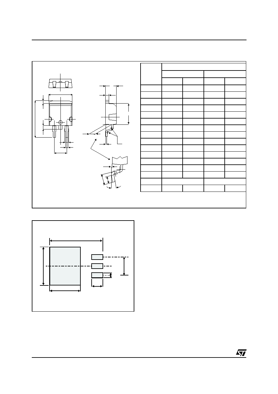
PACKAGE MECHANICAL DATA
D
2
PAK
A
C2
D
R
A2
M
V2
C
A1
G
L
L3
L2
B
B2
E
*
* FLAT ZONE NO LESS THAN 2mm
REF.
DIMENSIONS
Millimeters
Inches
Min.
Max.
Min.
Max.
A
4.40
4.60
0.173
0.181
A1
2.49
2.69
0.098
0.106
A2
0.03
0.23
0.001
0.009
B
0.70
0.93
0.027
0.037
B2
1.14
1.70
0.045
0.067
C
0.45
0.60
0.017
0.024
C2
1.23
1.36
0.048
0.054
D
8.95
9.35
0.352
0.368
E
10.00
10.40
0.393
0.409
G
4.88
5.28
0.192
0.208
L
15.00
15.85
0.590
0.624
L2
1.27
1.40
0.050
0.055
L3
1.40
1.75
0.055
0.069
M
2.40
3.20
0.094
0.126
R
0.40 typ.
0.016 typ.
V2
0∞
8∞
0∞
8∞
8.90
3.70
1.30
5.08
16.90
10.30
FOOT PRINT DIMENSIONS (in millimeters)
STPS20L15D/G
4/5

Information furnished is believed to be accurate and reliable. However, STMicroelectronics assumes no responsibility for the consequences of
use of such information nor for any infringement of patents or other rights of third parties which may result from its use. No license is granted by
implication or otherwise under any patent or patent rights of STMicroelectronics. Specifications mentioned in this publication are subject to
change without notice. This publication supersedes and replaces all information previously supplied.
STMicroelectronics products are not authorized for use as critical components in life support devices or systems without express written ap-
proval of STMicroelectronics.
The ST logo is a registered trademark of STMicroelectronics
© 1999 STMicroelectronics - Printed in Italy - All rights reserved.
STMicroelectronics GROUP OF COMPANIES
Australia - Brazil - China - Finland - France - Germany - Hong Kong - India - Italy - Japan - Malaysia
Malta - Morocco - Singapore - Spain - Sweden - Switzerland - United Kingdom - U.S.A.
http://www.st.com
PACKAGE MECHANICAL DATA
TO-220AC
A
C
D
E
M
L7
H2
ÿ I
L5
L6
L9
L4
G
F1
F
L2
REF.
DIMENSIONS
Millimeters
Inches
Min.
Max.
Min.
Max.
A
4.40
4.60
0.173
0.181
C
1.23
1.32
0.048
0.051
D
2.40
2.72
0.094
0.107
E
0.49
0.70
0.019
0.027
F
0.61
0.88
0.024
0.034
F1
1.14
1.70
0.044
0.066
G
4.95
5.15
0.194
0.202
H2
10.00
10.40
0.393
0.409
L2
16.40 typ.
0.645 typ.
L4
13.00
14.00
0.511
0.551
L5
2.65
2.95
0.104
0.116
L6
15.25
15.75
0.600
0.620
L7
6.20
6.60
0.244
0.259
L9
3.50
3.93
0.137
0.154
M
2.6 typ.
0.102 typ.
Diam. I
3.75
3.85
0.147
0.151
Ordering type
Marking
Package
Weight
Base qty
Delivery mode
STPS20L15D
STPS20L15D
TO-220AC
1.86 g.
50
Tube
STPS20L15G
STPS20L15G
D
2
PAK
1.48g.
50
Tube
STPS20L15G-TR
STPS20L15G
D
2
PAK
1.48 g.
1000
Tape and reel
Cooling method: by conduction (C)
Recommended torque value: 0.55 m.N
Maximum torque value: 0.7 m.N
Epoxy meets UL94,V0
STPS20L15D/G
5/5