 | –≠–ª–µ–∫—Ç—Ä–æ–Ω–Ω—ã–π –∫–æ–º–ø–æ–Ω–µ–Ω—Ç: P6KE15A | –°–∫–∞—á–∞—Ç—å:  PDF PDF  ZIP ZIP |
PEAK PULSE POWER : 600 W (10/1000
µ
s)
BREAKDOWN VOLTAGE RANGE :
From 6.8V to 440 V.
UNI AND BIDIRECTIONAL TYPES.
LOW CLAMPING FACTOR.
FAST RESPONSE TIME.
UL RECOGNIZED.
FEATURES
CB417
Symbol
Parameter
Value
Unit
P
PP
Peak pulse power dissipation (see note 1)
Tj initial =T
amb
600
W
P
Power dissipation on infinite heatsink
T
amb
= 75
∞
C
5
W
I
FSM
Non repetitive surge peak forward current
For Unidirectional types.
Tj initial =T
amb
tp =10 ms
100
A
T
stg
T
j
Storage temperature range
Maximum junction temperature
- 65 to + 175
175
∞
C
∞
C
T
L
Maximum lead temperature for soldering during 10s at 5mm
from case
230
∞
C
Note 1 : For a surge greater than the maximum values, the diode will fail in short-circuit.
ABSOLUTE MAXIMUM RATINGS (Tamb = 25
∞
C)
DESCRIPTION
Transil diodes provide high overvoltage protection
by clamping action. Their instantaneous response
to transient overvoltages makes them particularly
suited to protect voltage sensitive devices such as
MOS Technology and low voltage supplied IC's.
November 1998 - Ed: 2A
P6KE6V8A/440A
P6KE6V8CA/440CA
Æ
TRANSIL
TM
Symbol
Parameter
Value
Unit
R
th
(j-l)
Junction-leads
20
∞
C/W
R
th
(j-a)
Junction to ambient on printed circuit.
L
lead
= 10 mm
75
∞
C/W
THERMAL RESISTANCES
1/6
I
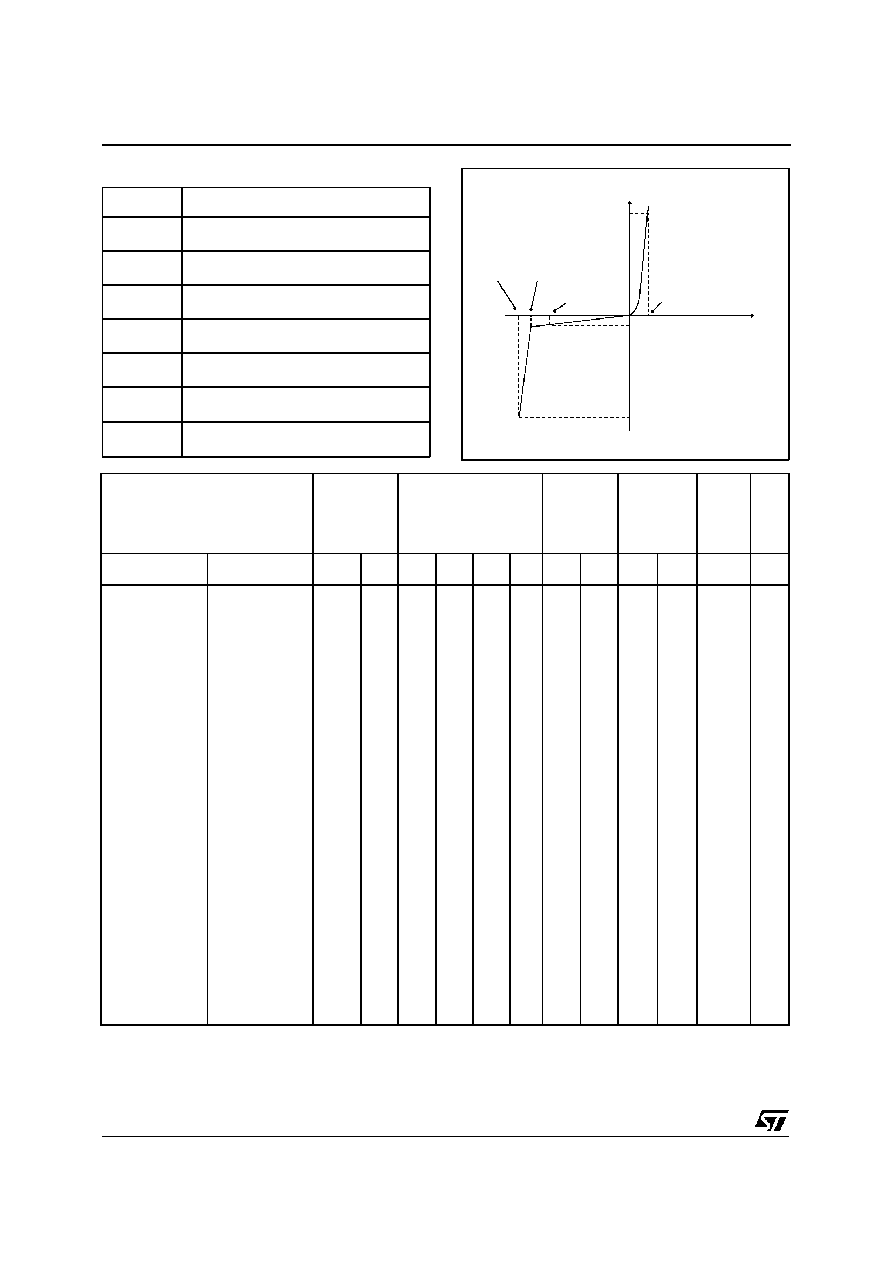
I F
VF
V
VCL
VBR
VRM
I PP
I RM
V
Symbol
Parameter
V
RM
Stand-off voltage.
V
BR
Breakdown voltage.
V
CL
Clamping voltage.
I
RM
Leakage current @ V
RM
.
I
PP
Surge current.
T
Voltage temperature coefficient.
V
F
Forward Voltage drop.
ELECTRICAL CHARACTERISTICS (Tamb = 25
∞
C)
TYPES
I
RM
@ V
RM
V
BR
@
I
R
V
CL
@ I
PP
V
CL
@ I
PP
T
C
max
min
nom
max
max
max
max
typ
note2
10/1000
µ
s
8/20
µ
s
note3
note4
Unidirectional
Bidirectional
µ
A
V
V
V
V
mA
V
A
V
A
10
-4
/
∞
C
pF
P6KE6V8A
P6KE6.8CA
1000
5.8
6.45
6.8
7.14
10
10.5
57
13.4
298
5.7
4000
P6KE7V5A
P6KE7.5CA
500
6.4
7.13
7.5
7.88
10
11.3
53
14.5
276
6.1
3700
P6KE10A
P6KE10CA
10
8.55
9.5
10
10.5
1
14.5
41
18.6
215
7.5
2800
P6KE12A
P6KE12CA
5
10.2
11.4
12
12.6
1
16.7
36
21.7
184
7.8
2300
P6KE15A
P6KE15CA
1
12.8
14.3
15
15.8
1
21.2
28
27.2
147
8.4
1900
P6KE18A
P6KE18CA
1
15.3
17.1
18
18.9
1
25.2
24
32.5
123
8.8
1600
P6KE22A
P6KE22CA
1
18.8
20.9
22
23.1
1
30.6
20
39.3
102
9.2
1350
P6KE24A
P6KE24CA
1
20.5
22.8
24
25.2
1
33.2
18
42.8
93
9.4
1250
P6KE27A
P6KE27CA
1
23.1
28.7
27
28.4
1
37.5
16
48.3
83
9.6
1150
P6KE30A
P6KE30CA
1
25.6
28.5
30
31.5
1
41.5
14.5
53.5
75
9.7
1075
P6KE33A
P6KE33CA
1
28.2
31.4
33
24.7
1
45.7
13.1
59
68
9.8
1000
P6KE36A
P6KE36CA
1
30.8
34.2
36
37.8
1
49.9
12
64.3
62
9.9
950
P6KE39A
P6KE39CA
1
33.3
37.1
39
41.0
1
53.9
11.1
69.7
57
10.0
900
P6KE47A
P6KE47CA
1
40.2
44.7
47
49.4
1
64.8
9.3
84
48
10.1
800
P6KE56A
P6KE56CA
1
47.8
53.2
56
58.8
1
77
7.8
100
40
10.3
700
P6KE68A
P6KE68CA
1
58.1
64.6
68
71.4
1
92
6.5
121
33
10.4
625
P6KE82A
P6KE82CA
1
70.1
77.9
82
86.1
1
113
5.3
146
27
10.5
550
P6KE100A
P6KE100CA
1
85.5
95.0
100
105
1
137
4.4
178
22.5
10.6
500
P6KE120A
P6KE120CA
1
102
114
120
126
1
165
3.6
212
19
10.7
450
P6KE150A
P6KE150CA
1
128
143
150
158
1
207
2.9
265
15
10.8
400
P6KE180A
P6KE180CA
1
154
171
180
189
1
246
2.4
317
12.6
10.8
360
P6KE200A
P6KE200CA
1
171
190
200
210
1
274
2.2
353
11.3
10.8
350
P6KExx
2/6

TYPES
I
RM
@ V
RM
V
BR
@
I
R
V
CL
@ I
PP
V
CL
@ I
PP
T
C
max
min
nom
max
max
max
max
typ
note2
10/1000
µ
s
8/20
µ
s
note3
note4
Unidirectional
Bidirectional
µ
A
V
V
V
V
mA
V
A
V
A
10
-4
/
∞
C
pF
P6KE220A
P6KE220CA
1
188
209
220
231
1
328
2
388
10.3
10.8
330
P6KE250A
P6KE250CA
1
213
237
250
263
1
344
2
442
9
11
310
P6KE300A
P6KE300CA
1
256
285
300
315
1
414
1.6
529
7.6
11
290
P6KE350A
P6KE350CA
1
299
332
350
368
1
482
1.6
618
6.5
11
270
P6KE400A
P6KE400CA
1
342
380
400
420
1
548
1.3
706
5.7
11
360
P6KE440A
P6KE440CA
1
376
418
440
462
1
603
1.3
776
5.2
11
350
Note 2 :
Pulse test : tp < 50 ms.
Note 3 :
V
BR
=
T
*
(Ta - 25)
*
V
BR
(25
∞
C).
Note 4
V
R
= 0 V, F = 1 MHz. For bidirectional types,
capacitance value is divided by 2.
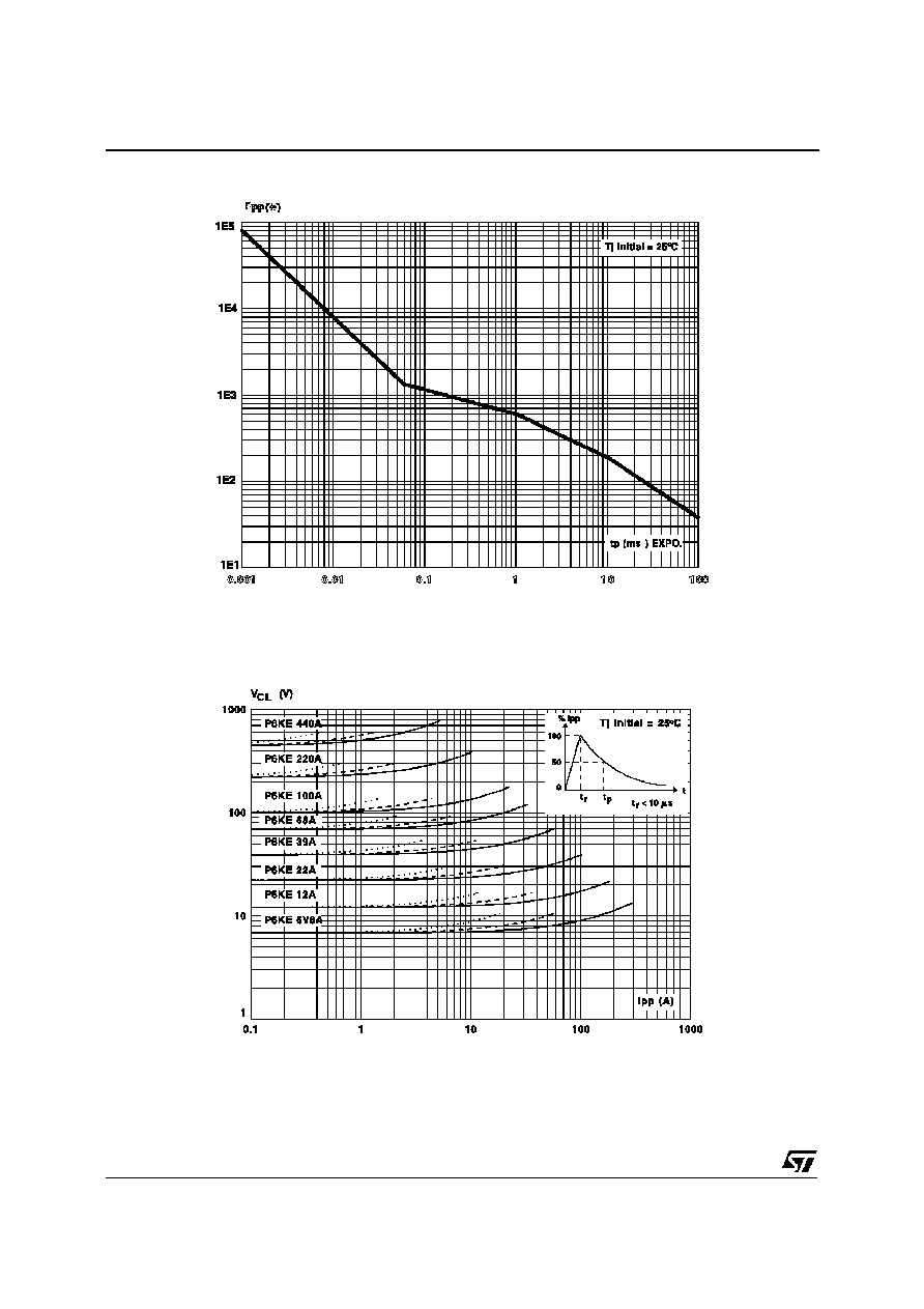
Fig 1: Peak pulse power dissipation versus initial
junction temperature (printed circuit board).
10 s
1000
s
% I
PP
50
0
t
PUL SE WAVEFORM 10/1000
s
100
P6KExx
3/6
0.001
0.01
0 .1
1
10
100
Ppp (W)
Fig. 2 : Peak pulse power versus exponential pulse duration.
Fig. 3 : Clamping voltage versus peak pulse current.
exponential waveform : t p = 20
µ
s________
t p = 1 ms-------------
t p =10 ms ...............
Note : The curves of the figure 3 are specified for a junction temperature of 25
∞
C before surge.
The given results may be extrapolated for other junction temperatures by using the following formula :
V
(BR)
=
T
(V(BR)) *
[T
a
-25]
*
V
(BR)
.
For intermediate voltages, extrapolate the given results.
P6KExx
4/6
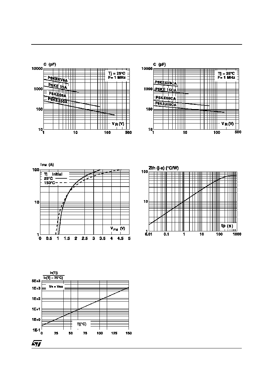
Fig. 6 : Transient thermal impedance junction-am-
bient versus pulse duration (For FR4 PC Board
with L
lead
= 10mm).
Fig. 5 : Peak forward voltage drop versus peak
forward current (typical values for unidirectional
types).
Fig. 4b : Capacitance versus reverse applied
voltage for bidirectional types (typical values).
Fig. 4a : Capacitance versus reverse applied
voltage for unidirectional types (typical values).
Note : multiply by 2 for units with VBR > 220 V.
Fig. 7 : Relative variation of leakage current
versus junction temperature.
P6KExx
5/6