Æ
1/10
SMP100MC
TRISILTM FOR TELECOM EQUIPMENT PROTECTION
REV. 1
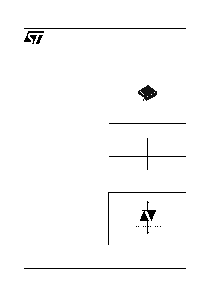
SMB
(JEDEC DO-214AA)
December 2004
FEATURES
Bidirectional crowbar protection
Voltage: range from 120V to 270V
Low V
BO
/ V
R
ratio
Micro capacitance from 20pF to 30pF @ 50V
Low leakage current : I
R
= 2µA max
Holding current: I
H
= 150 mA min
Repetitive peak pulse current :
I
PP
= 100 A (10/1000µs)
MAIN APPLICATIONS
Any sensitive equipment requiring protection
against lightning strikes and power crossing.
These devices are dedicated to central office pro-
tection as they comply with the most stressfull
standards.
Their Micro Capacitance make them suitable for
ADSL2+ and low end VDSL.
DESCRIPTION
The SMP100MC is a series of micro capacitance
transient surge arrestors designed for the protec-
tion of high debit rate communication equipment.
Its micro capacitance avoids any distortion of the
signal and is compatible with digital transmission
line cards (ADSL, VDSL, ISDN...).
Compatible with Cooper Bussmann fuse:
TCP 1.25A.
BENEFITS
Trisils are not subject to ageing and provide a fail
safe mode in short circuit for a better protection.
They are used to help equipment to meet main
standards such as UL60950, IEC950 / CSA C22.2
and UL1459. They have UL94 V0 approved resin.
SMB package is JEDEC registered (DO-214AA).
Trisils comply with the following standards GR-
1089 Core, ITU-T-K20/K21, VDE0433, VDE0878,
IEC61000-4-5 and FCC part 68.
Table 1: Order Codes
Part Number
Marking
SMP100MC-120
ML12
SMP100MC-140
ML14
SMP100MC-160
ML16
SMP100MC-200
ML20
SMP100MC-230
ML23
SMP100MC-270
ML27
Figure 1: Schematic Diagram

SMP100MC
2/10
Table 2: In compliance with the following standards
Table 3: Absolute Ratings (T
amb
= 25∞C)
STANDARD
Peak Surge
Voltage
(V)
Waveform
Voltage
Required
peak current
(A)
Current
waveform
Minimum serial
resistor to meet
standard (
)
GR-1089 Core
First level
2500
1000
2/10 µs
10/1000 µs
500
100
2/10 µs
10/1000 µs
0
0
GR-1089 Core
Second level
5000
2/10 µs
500
2/10 µs
0
GR-1089 Core
Intra-building
1500
2/10 µs
100
2/10 µs
0
ITU-T-K20/K21
6000
1500
10/700 µs
150
37.5
5/310 µs
0
0
ITU-T-K20
(IEC61000-4-2)
8000
15000
1/60 ns
ESD contact discharge
ESD air discharge
0
0
VDE0433
4000
2000
10/700 µs
100
50
5/310 µs
0
0
VDE0878
4000
2000
1.2/50 µs
100
50
1/20 µs
0
0
IEC61000-4-5
4000
4000
10/700 µs
1.2/50 µs
100
100
5/310 µs
8/20 µs
0
0
FCC Part 68, lightning
surge type A
1500
800
10/160 µs
10/560 µs
200
100
10/160 µs
10/560 µs
0
0
FCC Part 68, lightning
surge type B
1000
9/720 µs
25
5/320 µs
0
Symbol
Parameter
Value
Unit
I
PP
Repetitive peak pulse current
10/1000 µs
8/20 µs
10/560 µs
5/310 µs
10/160 µs
1/20 µs
2/10 µs
100
400
140
150
200
400
500
A
I
FS
Fail-safe mode : maximum current (note 1)
8/20 µs
5
kA
I
TSM
Non repetitive surge peak on-state current (sinusoidal)
t = 0.2 s
t = 1 s
t = 2 s
t = 15 mn
18
9
7
4
A
I
2
t
I
2
t value for fusing
t = 16.6 ms
t = 20 ms
20
21
A
2
s
T
stg
T
j
Storage temperature range
Maximum junction temperature
-55 to 150
150
∞C
T
L
Maximum lead temperature for soldering during 10 s.
260
∞C
Note 1: in fail safe mode, the device acts as a short circuit

SMP100MC
3/10
Table 4: Thermal Resistances
Table 5: Electrical Characteristics (T
amb
= 25∞C)
Symbol
Parameter
Value
Unit
R
th(j-a)
Junction to ambient (with recommended footprint)
100
∞C/W
R
th(j-l)
Junction to leads
20
∞C/W
Symbol
Parameter
V
RM
Stand-off voltage
V
BR
Breakdown voltage
V
BO
Breakover voltage
I
RM
Leakage current
I
PP
Peak pulse current
I
BO
Breakover current
I
H
Holding current
V
R
Continuous reverse voltage
I
R
Leakage current at V
R
C
Capacitance
Types
I
RM
@ V
RM
I
R
@ V
R
Dynamic
V
BO
Static
V
BO
@ I
BO
I
H
C
C
max.
max.
max.
max.
max.
min.
typ.
typ.
note1
note 2
note 3
note 4 note 5 note 6
µA
V
µA
V
V
V
mA
mA
pF
pF
SMP100MC-120*
2
108
5
120
155
150
800
150
30
60
SMP100MC-140*
126
140
180
175
30
60
SMP100MC-160
144
160
205
200
25
50
SMP100MC-200
180
200
255
250
20
45
SMP100MC-230
207
230
295
285
20
40
SMP100MC-270
243
270
345
335
20
40
Note 1: IR measured at VR guarantee VBR min
VR
Note 2: see functional test circuit 1
Note 3: see test circuit 2
Note 4: see functional holding current test circuit 3
Note 5: VR = 50V bias, VRMS=1V, F=1MHz
Note 6: VR = 2V bias, VRMS=1V, F=1MHz
* in development
SMP100MC
4/10
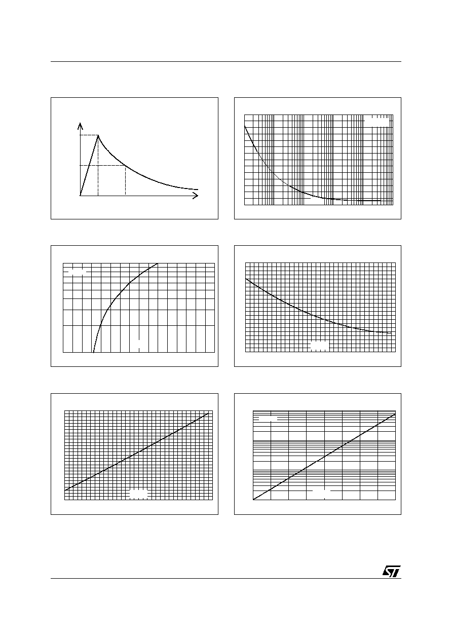
Figure 2: Pulse waveform
Figure 3: Non repetitive surge peak on-state
current versus overload duration
Figure 4: On-state voltage versus on-state
current (typical values)
Figure 5: Relative variation of holding current
versus junction temperature
Figure 6: Relative variation of breakover
voltage versus junction temperature
Figure 7: Relative variation of leakage current
versus junction temperature (typical values)
100
50
%I
PP
t
r
t
p
0
t
Repetitive peak pulse current
tr = rise time (µs)
tp = pulse duration time (µs)
0
10
20
30
40
50
60
70
1.E-02
1.E-01
1.E+00
1.E+01
1.E+02
1.E+03
I
(A)
TSM
t(s)
F=50Hz
Tj initial = 25∞C
10
100
0
1
2
3
4
5
6
7
8
V (V)
T
I (A)
T
Tj=25∞C
0.0
0.2
0.4
0.6
0.8
1.0
1.2
1.4
1.6
1.8
2.0
2.2
-40 -30 -20 -10
0
10
20
30
40
50
60
70
80
90 100 110 120 130
Tj(∞C)
I [Tj] / I [Tj=25∞C]
H
H
0.94
0.95
0.96
0.97
0.98
0.99
1.00
1.01
1.02
1.03
1.04
1.05
1.06
1.07
1.08
-40 -30 -20 -10
0
10
20
30
40
50
60
70
80
90 100 110 120 130
Tj(∞C)
V
[Tj] / V
[Tj=25∞C]
BO
BO
1.E+00
1.E+01
1.E+02
1.E+03
25
50
75
100
125
I [Tj] / I [Tj=25∞C]
R
R
Tj(∞C)
V =243V
R

SMP100MC
5/10
APPLICATION NOTE
Figure 8: Variation of thermal impedance
junction to ambient versus pulse duration
(Printed circuit board FR4, SCu=35µm,
recommended pad layout)
Figure 9: Relative variation of junction
capacitance versus reverse voltage applied
(typical values)
In wireline applications, analog or digital, both central office and subscriber sides have to be protected.
This function is assumed by a combined series / parallel protection stage.
In such a stage, parallel function is assumed by one or several Trisil, and is used to protect against short
duration surge (lightning). During this kind of surges the Trisil limits the voltage across the device to be
protected at its break over value and then fires. The fuse assumes the series function, and is used to pro-
tect the module against long duration or very high current mains disturbances (50/60Hz). It acts by safe
circuits opening. Lightning surge and mains disturbance surges are defined by standards like GR1089,
FCC part 68, ITU-T K20.
0.0
0.1
0.2
0.3
0.4
0.5
0.6
0.7
0.8
0.9
1.0
1.E-02
1.E-01
1.E+00
1.E+01
1.E+02
1.E+03
tp(s)
Z
/R
th(j-a)
th(j-a)
0.0
0.1
0.2
0.3
0.4
0.5
0.6
0.7
0.8
0.9
1.0
1.1
1.2
1
10
100
1000
V (V)
R
C [V ] / C [V =2V]
R
R
F =1MHz
V
= 1V
Tj = 25∞C
OSC
RMS
Line
Protection stage
Protection stage
Ring
relay
Line
Ex. Analog line card
Ex. ADSL line card or terminal
Fuse TCP 1.25A
T1
T2
SMP100MC-xxx
Fuse TCP 1.25A
Tip S
Gnd
SMP100MC-xxx
Ring S
SMP100MC-xxx
Fuse TCP 1.25A
Tip L
Gnd
Ring L
Typical circuit for subscriber side
Typical circuit for central office side