
Æ
1/9
SMP80MC
TRISILTM FOR TELECOM EQUIPMENT PROTECTION
REV. 3
SMB
(JEDEC DO-214AA)
June 2005
FEATURES
Bidirectional crowbar protection
Voltage: range from 120V to 270V
Low V
BO
/ V
R
ratio
Micro capacitance equal to 12pF @ 50V
Low leakage current : I
R
= 2µA max
Holding current: I
H
= 150 mA min
Repetitive peak pulse current :
I
PP
= 80 A (10/1000µs)
MAIN APPLICATIONS
Any sensitive equipment requiring protection
against lightning strikes and power crossing:
Terminals (phone, fax, modem...) and central
office equipment
DESCRIPTION
The SMP80MC is a series of micro capacitance
transient surge arrestors designed for the protec-
tion of high debit rate communication equipment
on CPE side. Its micro capacitance avoids any dis-
tortion of the signal and is compatible with digital
transmission like ADSL2 and ADSL2+.
BENEFITS
Trisils are not subject to ageing and provide a fail
safe mode in short circuit for a better protection.
They are used to help equipment to meet main
standards such as UL1950, IEC950 / CSA C22.2
and UL1459. They have UL94 V0 approved resin.
SMB package is JEDEC registered (DO-214AA).
Trisils comply with the following standards GR-
1089 Core, ITU-T-K20/K21, VDE0433, VDE0878,
IEC61000-4-5 and FCC part 68.
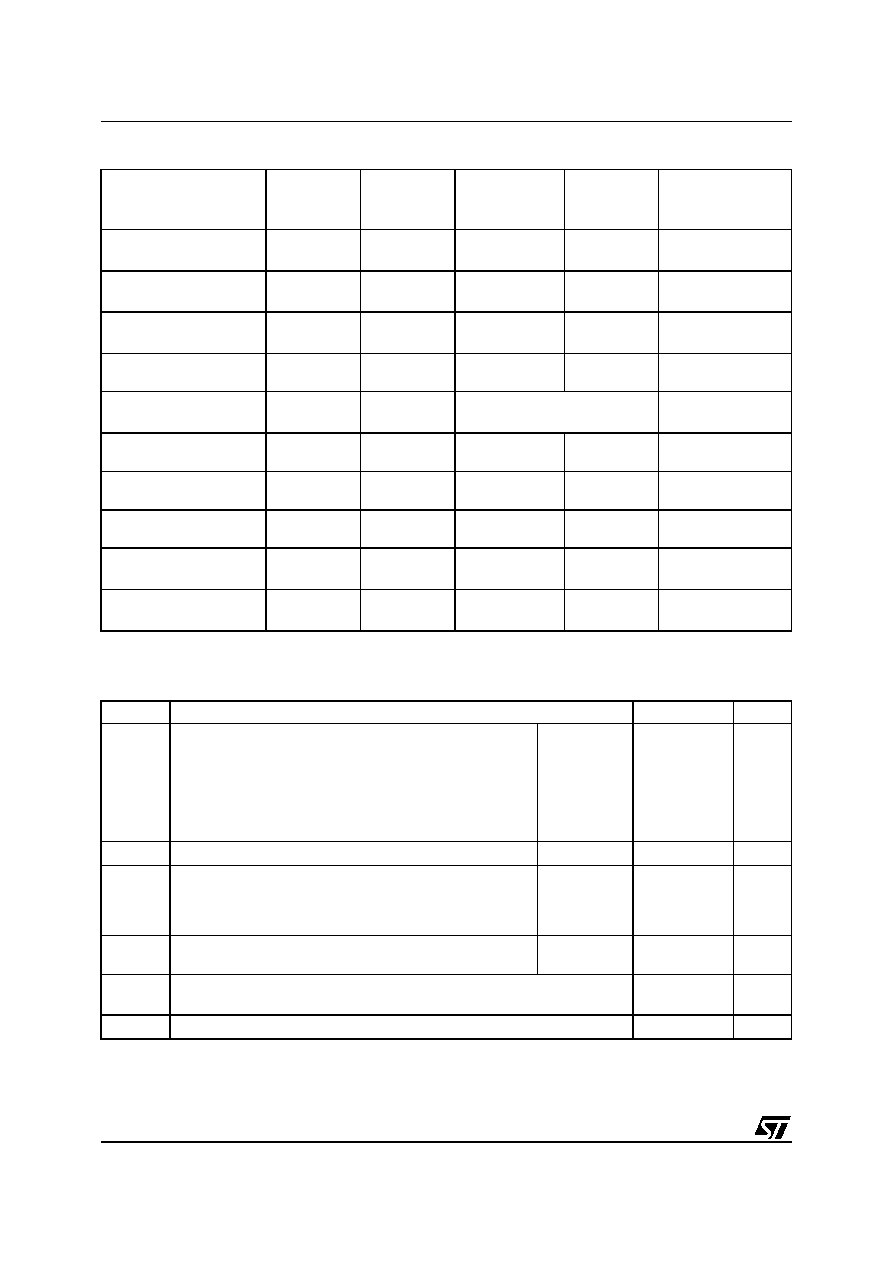
Table 1: Order Codes
Part Number
Marking
SMP80MC-120
TP12
SMP80MC-140
TP14
SMP80MC-160
TP16
SMP80MC-200
TP20
SMP80MC-230
TP23
SMP80MC-270
TP27
Figure 1: Schematic Diagram
TM: TRISIL is a trademark of STMicroelectronics.
SMP80MC
2/9
Table 2: In compliances with the following standards
Table 3: Absolute Ratings (T
amb
= 25∞C)
STANDARD
Peak Surge
Voltage
(V)
Waveform
Voltage
Required
peak current
(A)
Current
waveform
Minimum serial
resistor to meet
standard (
)
GR-1089 Core
First level
2500
1000
2/10 µs
10/1000 µs
500
100
2/10 µs
10/1000 µs
5
2.5
GR-1089 Core
Second level
5000
2/10 µs
500
2/10 µs
10
GR-1089 Core
Intra-building
1500
2/10 µs
100
2/10 µs
0
ITU-T-K20/K21
6000
1500
10/700 µs
150
37.5
5/310 µs
10
0
ITU-T-K20
(IEC61000-4-2)
8000
15000
1/60 ns
ESD contact discharge
ESD air discharge
0
0
VDE0433
4000
2000
10/700 µs
100
50
5/310 µs
0
0
VDE0878
4000
2000
1.2/50 µs
100
50
1/20 µs
0
0
IEC61000-4-5
4000
4000
10/700 µs
1.2/50 µs
100
100
5/310 µs
8/20 µs
0
0
FCC Part 68, lightning
surge type A
1500
800
10/160 µs
10/560 µs
200
100
10/160 µs
10/560 µs
2.5
0
FCC Part 68, lightning
surge type B
1000
9/720 µs
25
5/320 µs
0
Symbol
Parameter
Value
Unit
I
PP
Repetitive peak pulse current (see figure 2)
10/1000 µs
8/20 µs
10/560 µs
5/310 µs
10/160 µs
1/20 µs
2/10 µs
80
200
100
120
150
200
250
A
I
FS
Fail-safe mode : maximum current (note 1)
8/20 µs
5
kA
I
TSM
Non repetitive surge peak on-state current (sinusoidal)
t = 0.2 s
t = 1 s
t = 2 s
t = 15 mn
14
8
6.5
2
A
I
2
t
I
2
t value for fusing
t = 16.6 ms
t = 20 ms
7.5
7.8
A
2
s
T
stg
T
j
Storage temperature range
Maximum junction temperature
-55 to 150
150
∞C
T
L
Maximum lead temperature for soldering during 10 s.
260
∞C
Note 1: in fail safe mode, the device acts as a short circuit

SMP80MC
3/9
Table 4: Thermal Resistances
Table 5: Electrical Characteristics (T
amb
= 25∞C)
Symbol
Parameter
Value
Unit
R
th(j-a)
Junction to ambient (with recommended footprint)
100
∞C/W
R
th(j-l)
Junction to leads
20
∞C/W
Symbol
Parameter
V
RM
Stand-off voltage
V
BR
Breakdown voltage
V
BO
Breakover voltage
I
RM
Leakage current
I
PP
Peak pulse current
I
BO
Breakover current
I
H
Holding current
V
R
Continuous reverse voltage
I
R
Leakage current at V
R
C
Capacitance
Types
I
RM
@ V
RM
I
R
@ V
R
Dynamic
V
BO
Static
V
BO
@ I
BO
I
H
C
C
max.
max.
max.
max.
max.
min.
typ.
typ.
note1
note 2
note 3
note 4 note 5 note 6
µA
V
µA
V
V
V
mA
mA
pF
pF
SMP80MC-120
2
108
5
120
155
155
800
150
12
25
SMP80MC-140
126
140
180
180
SMP80MC-160
144
160
205
205
SMP80MC-200
180
200
255
255
SMP80MC-230
207
230
295
295
SMP80MC-270
243
270
345
345
Note 1: IR measured at VR guarantee VBR min
VR
Note 2: see functional test circuit 1
Note 3: see test circuit 2
Note 4: see functional holding current test circuit 3
Note 5: VR = 50V bias, VRMS=1V, F=1MHz
Note 6: VR = 2V bias, VRMS=1V, F=1MHz

SMP80MC
4/9
Figure 2: Pulse waveform
Figure 3: Non repetitive surge peak on-state
current versus overload duration
Figure 4: On-state voltage versus on-state
current (typical values)
Figure 5: Relative variation of holding current
versus junction temperature
Figure 6: Relative variation of breakover
voltage versus junction temperature
Figure 7: Relative variation of leakage current
versus junction temperature (typical values)
100
50
% I
PP
t
t
r
p
0
t
Repetitive peak pulse current
tr = rise time (µs)
tp = pulse duration time (µs)
I
(A)
TSM
0
5
10
15
20
25
30
35
40
1.E-02
1.E-01
1.E+00
1.E+01
1.E+02
1.E+03
t(s)
F=50Hz
Tj initial = 25∞C
I (A)
T
10
100
0
1
2
3
4
5
6
7
8
Tj=25∞C
V (V)
T
I [Tj] / I [Tj=25∞C]
H
H
0.0
0.2
0.4
0.6
0.8
1.0
1.2
1.4
1.6
1.8
2.0
-40 -30 -20 -10
0
10
20
30
40
50
60
70
80
90 100 110 120 130
Tj(∞C)
V
[Tj] / V
[Tj=25∞C]
BO
BO
0.94
0.95
0.96
0.97
0.98
0.99
1.00
1.01
1.02
1.03
1.04
1.05
1.06
1.07
1.08
-40 -30 -20 -10
0
10
20
30
40
50
60
70
80
90 100 110 120 130
Tj(∞C)
I [Tj] / I [Tj=25∞C]
R
R
1.E+00
1.E+01
1.E+02
1.E+03
25
50
75
100
125
Tj(∞C)
V =243V
R

SMP80MC
5/9
Figure 8: Variation of thermal impedance
junction to ambient versus pulse duration
(Printed circuit board FR4, SCu=35µm,
recommended pad layout)
Figure 9: Relative variation of junction
capacitance versus reverse voltage applied
(typical values)
Figure 10: Test circuit 1 for dynamic I
BO
and V
BO
parameters
Z
/R
th(j-a)
th(j-a)
0.0
0.1
0.2
0.3
0.4
0.5
0.6
0.7
0.8
0.9
1.0
1.E-02
1.E-01
1.E+00
1.E+01
1.E+02
1.E+03
tp(s)
C [V ] / C [V =2V]
R
R
0.0
0.1
0.2
0.3
0.4
0.5
0.6
0.7
0.8
0.9
1.0
1.1
1.2
1
10
100
1000
V (V)
R
F =1MHz
V
= 1V
Tj = 25∞C
OSC
RMS
100 V / µs, di /dt < 10 A / µs, Ipp = 80 A
1 kV / µs, di /dt < 10 A / µs, Ipp = 10 A
U
U
10 µF
2
45
66
470
83
0.36 nF
46 µH
60 µF
26 µH
12
250
46 µH
47
KeyTek 'System 2' generator with PN246I module
KeyTek 'System 2' generator with PN246I module