SO2222
SO2222A
SMALL SIGNAL NPN TRANSISTORS
s
SILICON EPITAXIAL PLANAR NPN
TRANSISTORS
s
MINIATURE PLASTIC PACKAGE FOR
APPLICATION IN SURFACE MOUNTING
CIRCUITS
s
MEDIUM CURRENT AF AMPLIFICATION
AND SWITCHING
s
PNP COMPLEMENTS ARE RESPECTIVELY
SO2907 AND SO2907A
INTERNAL SCHEMATIC DIAGRAM
March 1996
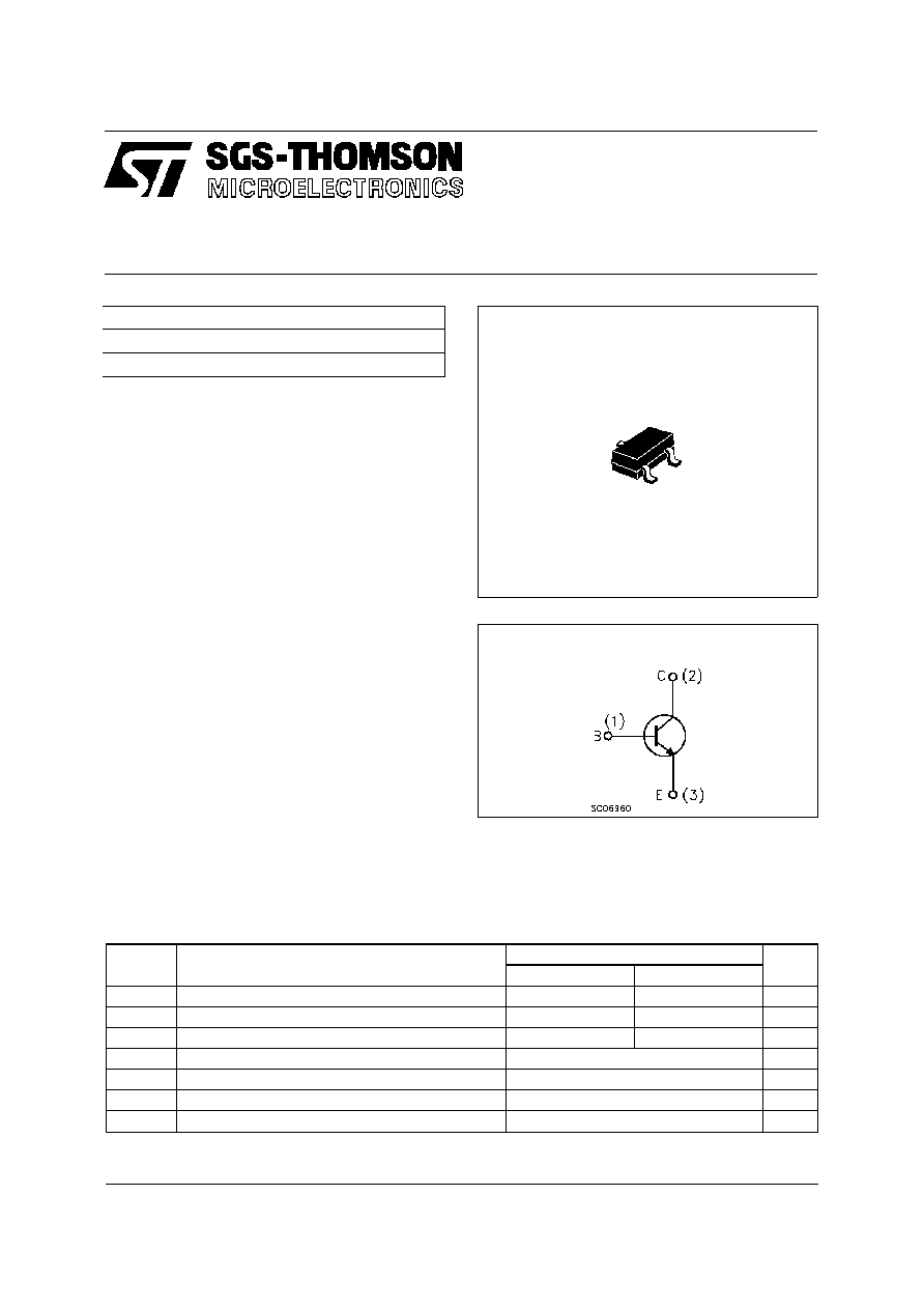
1
2
3
SOT-23
Type
Marking
SO2222
N13
SO 2222A
N20
ABSOLUTE MAXIMUM RATINGS
Symbol
Parameter
Val ue
Uni t
SO2222
SO 2222A
V
CBO
Collector-Emit ter Voltage (V
BE
= 0)
60
75
V
V
CEO
Collector-Emit ter Voltage (I
B
= 0)
30
40
V
V
EBO
Emitter-Base Voltage (I
C
= 0)
5
6
V
I
CM
Collector Peak Current
0.8
A
P
t ot
Tot al Dissipation at T
c
= 25
o
C
350
mW
T
stg
Storage Temperature
-65 to 150
o
C
T
j
Max. O perat ing Junction Temperature
150
o
C
1/5

THERMAL DATA
R
t hj-am b
∑
R
th j-SR
∑
Thermal Resistance Junction-Ambient
Max
Thermal Resistance Junction-Substrat e
Max
350
290
o
C/W
o
C/W
∑
Mounted on a ceramic substrate area = 15 x 15 x 0.6 mm
ELECTRICAL CHARACTERISTICS (T
case
= 25
o
C unless otherwise specified)
Symb ol
Parameter
Test Cond ition s
Mi n.
Typ .
Max.
Un it
I
CEX
Collect or Cut-off
Current (V
BE
= 0)
V
CE
= 60 V
V
BE
= -3 V
for SO2222A
10
nA
I
BEX
Base Cut-off Current
(V
BE
= 0)
V
CE
= 60 V
V
BE
= -3 V
for SO2222A
20
nA
I
CBO
Collect or Cut-off
Current (I
E
= 0)
V
CB
= rated V
CBO
V
CB
= rated V
CBO
T
j
= 150
o
C
10
10
nA
µ
A
I
EBO
Emitt er Cut-off Current
(I
C
= 0)
V
EB
= 3 V
for SO2222
for SO2222A
30
15
nA
nA
V
( BR)CEO
Collect or-Emitter
Breakdown Volt age
(I
B
= 0)
I
C
= 10 mA
for SO2222
for SO2222A
30
40
V
V
V
( BR)CBO
Collect or-Base
Breakdown Volt age
(I
B
= 0)
I
C
= 10
µ
A
for SO2222
for SO2222A
60
75
V
V
V
(BR)EBO
Emitt er-Base
Breakdown Volt age
(I
C
= 0)
I
E
= 10
µ
A
for SO2222
for SO2222A
5
6
V
V
V
CE(sat )
Collect or-Emitter
Saturat ion Voltage
I
C
= 150 mA
I
B
= 15 mA
for SO2222
for SO2222A
I
C
= 500 mA
I
B
= 50 mA
for SO2222
for SO2222A
0.4
0.3
1.6
1
V
V
V
V
V
BE(s at)
Collect or-Base
Saturat ion Voltage
I
C
= 150 mA
I
B
= 15 mA
for SO2222
for SO2222A
I
C
= 500 mA
I
B
= 50 mA
for SO2222
for SO2222A
0. 6
1.3
1.2
2.6
2
V
V
V
V
h
FE
DC Current G ain
I
C
= 0. 1 mA
V
CE
= 10 V
I
C
= 1 mA
V
CE
= 10 V
I
C
= 10 mA
V
CE
= 10 V
I
C
= 150 mA
V
CE
= 10 V
I
C
= 150 mA
V
CE
= 1 V
I
C
= 500 mA
V
CE
= 10 V
for SO2222
for SO2222A
35
50
75
100
50
30
40
300
f
T
Transit ion F requency
I
C
= 20 mA V
CE
= 20V f = 100MHz
for SO2222
for SO2222A
250
300
MHz
MHz
C
CB
Collect or Base
Capacitance
I
E
= 0
V
CB
= 10 V
f = 1 MHz
8
pF
Pulsed: Pulse duration = 300
µ
s, duty cycle
2 %
SO2222/SO2222A
2/5

Information furnished is believed to be accurate and reliable. However, SGS-THOMSON Microelectronics assumes no responsability for the
consequences of use of such information nor for any infringement of patents or other rights of third parties which may results from its use. No
license is granted by implication or otherwise under any patent or patent rights of SGS-THOMSON Microelectronics. Specifications mentioned
in this publication are subject to change without notice. This publication supersedes and replaces all information previously supplied.
SGS-THOMSON Microelectronics products are not authorized for use as critical components in life support devices or systems without express
written approval of SGS-THOMSON Microelectonics.
©
1995 SGS-THOMSON Microelectronics - Printed in Italy - All Rights Reserved
SGS-THOMSON Microelectronics GROUP OF COMPANIES
Australia - Brazil - Canada - China - France - Germany - Hong Kong - Italy - Japan - Korea - Malaysia - Malta - Morocco - The Netherlands -
Singapore - Spain - Sweden - Switzerland - Taiwan - Thailand - United Kingdom - U.S.A
.
SO2222/SO2222A
5/5

